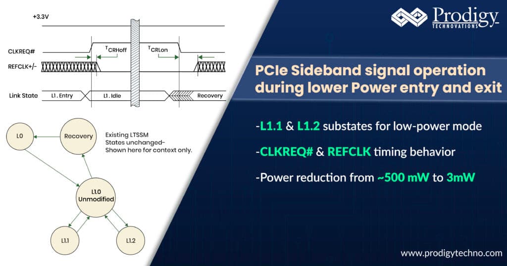
PCIe Sideband signal operation during lower Power entry and exit
In modern applications such as mobile devices, servers, gaming systems, and network storage, there is a growing demand for increased storage capacity. To meet this need, many of these devices are transitioning to solid-state drives (SSDs) using the NVMe protocol over PCIe. While PCIe has traditionally been considered a power-hungry interface, the PCI-SIG (PCI Special Interest Group) has been continuously evolving the PCIe specification to enhance performance while reducing power consumption, especially to support emerging, power-sensitive applications.
For battery-operated devices, it is critical to achieve fast wake-up times and longer battery life without fully powering down the device. Additionally, when the PCIe interface is idle, it must consume minimal power and be able to return to an active state seamlessly, without degrading the user experience.
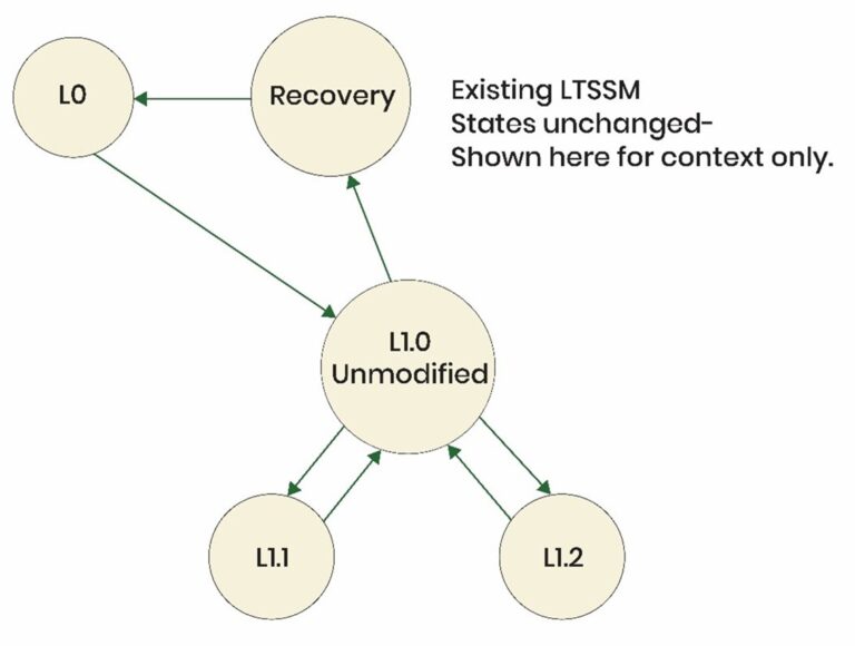
To address these requirements, PCI-SIG introduced L1 Substates (L1.1 and L1.2) as part of the PCIe power management architecture. These substates leverage the existing CLKREQ# signal, which is extended to support additional signaling for power control. This allows PCIe transceivers to power down their high-speed circuits during inactivity and use CLKREQ# to wake them up when needed.
With L1 Substates, power consumption can be reduced dramatically—from approximately 400–500 mW in the active L0 state to just 2–3 mW in L1.2, enabling significant power savings while maintaining responsiveness.
To ensure the interoperability between different root complex and end points the timing between to CLKREQ and REFCLK needs to be maintained. PCI-SIG recommends the timing values are
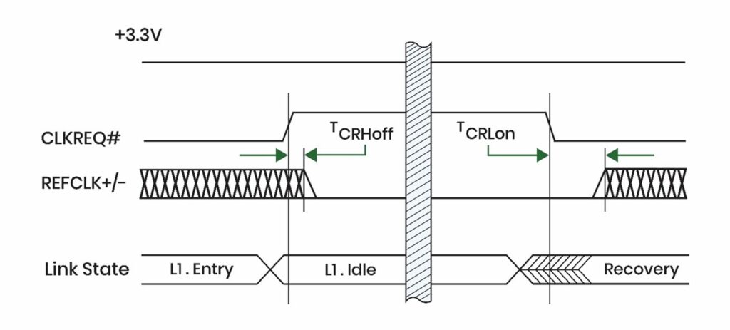
Power-Up CLKREQ# Timings
|
Symbol |
Parameter |
Min |
Max |
Units |
Note |
|
TCRHoff |
CLKREQ# de-asserted high to clock parked |
0 |
|
ns |
|
|
TCRLon |
CLKREQ# asserted low to clock active |
|
400 |
ns |
See note |
Note: TCRLon is allowed to exceed this value when LTR is supported and enabled for the device.The Latency Tolerance Reporting (LTR) mechanism allows a device to inform the host (Root Complex) about how long it can tolerate delays before its requests (such as interrupts or memory accesses) must be serviced. This helps the host coordinate power management and efficiently schedule servicing across multiple devices without compromising performance. LTR information is exchanged during the PCIe link-up phase, as part of the configuration and training sequence, allowing the host to make informed decisions on entering low-power states while still meeting device latency requirements.
Want to learn more? Join our webinar on “Overview of PCIe Sideband Signal Functionality at Power-On & Low Power State, and Validation.”
Register here: https://www.prodigytechno.com/overview-of-pcie-side-band-signals-functionalities-at-power-on-low-power-state-and-validation
Prodigy Technovations offers a PCIe Low Power Side Band Signal Analyzer to help you capture and analyze critical signal behavior during power transitions.
Learn more: https://www.prodigytechno.com/device/pcie-low-power-side-band-signal-analyzer
Keep up with the latest PCIe industry updates by visiting our PCIe News page.