MDIO (Management Data Input/Output)
Introduction to MDIO:
Management Data Input/Output (MDIO), or Media Independent Interface Management (MIIM) is a serial bus protocol defined for the IEEE 802.3 standard Ethernet series of Media Independent Interface (MII). MII connects media access control (MAC) devices to Ethernet physical layer (PHY) circuits. The SMI/MDIO protocol is a simple two-wire serial interface that connects the management unit to the managed PHY to control the PHY and capture the status of the PHY. The Management Data Input/Output (MDIO) component can be used to read and write the PHY control register. Each PHY can be monitored before operation and the connection status can be monitored during operation. These registers provide status and control information such as link status, speed ability, and selection, power down for low power consumption, duplex mode (full or half), auto-negotiation, fault signaling, and loopback. The main purpose of using MDIO protocol is to configure the PHY layer transceiver parameters, for example, PHY devices can perform pre-emphasis or de-emphasis in the Physical Coding Sublayer (PCS), programming the control status registers in the PHY layer.
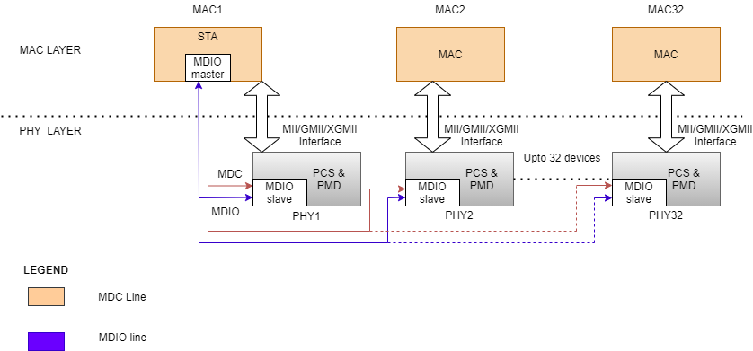
MDIO is a bidirectional shared bus structure that can provide a connection from the MAC (master) up to 32 PHY (slave) devices. All data is synchronously transmitted through the Management Data Clock (MDC), which is provided by the MAC and sent to all receiving devices. The data line is a tri-state shared bus that is MAC controlled for a write transaction or PHY controlled during a read transaction. The MDIO interface clock (MDC) supports frequencies up to 2.5MHz. The host processor, which is responsible for system configuration and monitoring, usually uses the MDIO host to perform individual access to various devices. MDIO was originally defined in Clause 22 of IEEE 802.3. To meet the growing needs of 10 Gigabit Ethernet devices, clause 45 of the 802.3ae specification is introduced.
MDIO System:
The MDIO bus has two signals: management data clock (MDC) and management data input/output (MDIO). MDIO has specific terms to define various devices on the bus. The device driving the MDIO bus is identified as a station management entity (STA). Target devices managed by MDC are called MDIO manageable devices (MMD). STA initiates all communications in MDIO and is responsible for controlling the clock on MDC. The specified frequency of MDC is up to 2.5 MHz. The following Figure captures the interface wiring diagram of a typical MDIO system.
Figure 1: Wiring diagram of a typical MDIO Application.
MDIO (SMI Protocol) Features:
- MDIO protocol has a configurable physical address.
- MDC (clock bus) is specified to have a frequency of up to 2.5 MHz.
- Capability added to address more registers–up to 65,536 registers in each device.
- Variable MDIO speeds and duty cycle.
- Power down for low power consumption.
MDIO Protocol Frame Format:
CLAUSE 22:
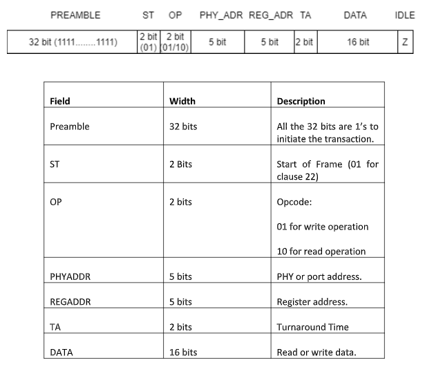
Figure 2: Clause 22 Frame format.
The MDIO data format for clause 22 is defined in the IEEE 802.3 Ethernet standard, as shown in the figure above.
Preamble (PRE): The first field in the MDIO protocol is indicated with Preamble. When the Preamble is sent, the MAC sends all bits as 1’s in the MDIO line. The 32 bits in the preamble are always 1’s.
Start (ST): The preamble is succeeded by the start bit which is 2 bits in size that remains 01 always in clause 22 for both read or write operations.
Opcode (OP): The next field is the opcode which gives information about whether a read or write operation is to be performed. Opcode with the value of ‘01’ in the frame specifies the write operation. Similarly, Opcode with the value of ‘10’ in the frame specifies read operation.
Physical Address (PHYAD): This field contains a 5-bit PHY address.
Register Address (REGAD): This field is 5 bits long indicating the register to be written or read from.
Turn Around (TA): The Turnaround field is 2 bits in size. When data is written to the PHY, the MAC will write “10” to the MDIO bus. When reading data, the MAC releases the MDIO bus.
Data: This field is 16-bit wide. During the read instruction, the PHY chip writes the data read from the REGAD register corresponding to the PHYAD in Data. During the write instruction, the MAC writes the value of the REGAD register corresponding to the PHYAD in Data.
Idle: At this state, MDIO is driven to a high impedance state, but it is generally pulled up with the help of a pull-up resistor.
CLAUSE 45:
Since there are not enough registers for future use, there was a need for Clause 45 to meet the growing need for 10-bit gigabit ethernet devices. There was little scope to cater multi the device’s PHY layer.
In addition, to read and write in Clause 22, additional commands are added in Clause 45. Clause 45 added support for low-voltage devices down to 1.2V and extended the frame format to provide access to many more devices and registers.
The MDIO data format for clause 45 is defined in the IEEE 802.3 Ethernet standard, as shown in the figure above.
The advantages of clause 45 over clause 22 are as follows:
- Accessibility of 65,536 registers in 32 different devices across 32 different ports.
- Additional OP and ST code for indirect access to register address for 10 Gigabit Ethernet.
- Terminal fault signaling. Multiple repeaters.
- Low voltage specification
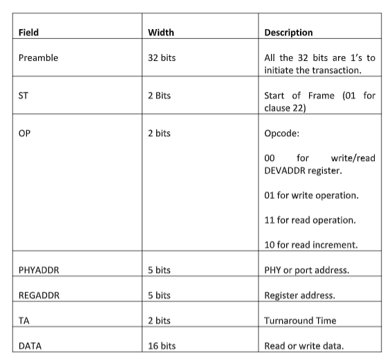
Figure 3: Clause 45 Frame Format
Preamble (PRE): The first field in the MDIO protocol is indicated with Preamble. When the Preamble is sent, the MAC sends all bits as 1’s in the MDIO line. The 32 bits in the preamble are always 1’s.
Start (ST): The preamble is succeeded by the start bit which is two bits in size that remain 00 always in clause 45 for all operations.
Opcode (OP): The next field is the opcode which gives information on whether a read or write operation is to be executed. Opcode with the value of ‘01’ in the frame specifies the write operation. The opcode with the value of 11 specifies the read operation. There exist additional two commands namely read increment and address. The read increment with opcode 10 does a read operation with the MMD device address incrementing after each access. The opcode with value 00 is to rewrite or reread DEV ADD’s address register.
Physical Address (PRTAD): This field consists of the 5-bit PHY address.
Device Address (REGAD): This field is 5 bits long indicating the registered address that must be written or read from.
Turn Around (TA): The Turnaround field is 2 bits in size. When data is written to the PHY, the MAC will write “10” to the MDIO line. When reading data, the MAC releases the MDIO bus to initiate driving read data if read operation.
Data: This field is 16-bit wide. During the read instruction, the PHY chip writes the data read from the REGAD register corresponding to the PHYAD in Data. During the write instruction, the MAC writes the value of the REGAD register corresponding to the PHYAD in Data.
Idle: At this state, the MDIO bus is driven to a high impedance state, but it is pulled up through a pull-up resistor of 1.5k ohm.
Theory of Operation:
The PHY devices require a preamble of 32 ones that must be sent by the MAC to PHY on the MDIO line. The register access consists of 16 control bits followed by 16 data bits. The control bits consist of 2 start bits, 2 bits for opcode or the type of operation (read or write), the PHY address (5 bits), the registered address (5 bits), and 2 turnaround bits. In a write instruction, the MAC provides the address and data. For a read instruction, the PHY receives from the MDIO stream during the turnaround, supplies the MAC with the requested register data, and then releases the MDIO stream.
When the MAC is driving the MDIO line, it must guarantee a steady value of 10 ns (setup time) before the rising edge of the MDC clock. In addition, the MDIO must remain stable for 10 ns (hold time) after the rising edge of the MDC. When the PHY drives the MDIO line, the PHY must provide an MDIO signal between 0 and 300 ns after the rising edge of the clock.
Therefore, with a minimum clock interval of 400 ns (max clock rate is 2.5 MHz), the MAC can safely sample the MDIO during the second half of the low clock cycle. The entire MDIO line is sampled on the rising edge of the clock except for the read operation. During the read operation, the MDIO line is sampled on the falling edge of the clock.
Figure 4: Theory of operation for clause 22.
Once the preamble is sent, the next two bits indicate the start operation. The start field is followed by a read or write operation. The corresponding PHY address is then sent on the MDIO line. The registered address of the PHY is then sent to the MDIO line. Both the addresses are 5 bits wide. During the turnaround, When the data is written to PHY, the MAC sends “10” indicating the line is free for the data to be written.
During the read operation, The MAC releases the MDIO line. The data is sampled during the read operation on the falling edge of the clock. If there is a mismatch with the PHY address, The value after the TA field will be continuously high. This means to say that MAC is trying to write to the register that does not exist.
Since there is a limit to using only 5-bit addresses for both PHYADDR and REGADDR, it limits the number of MMDs the STA can communicate with. Also, MDIO clause 22 only supports 5V tolerant devices and there is no low voltage option.
The main change in Clause 45 is how the registers are accessed. In Clause 22, both the address and read or write data are specified in one frame. Clause 45 changes this paradigm. First, an address frame indicating the MMD and the register is sent. Then a second read or write frame is sent.
An advantage of adding this two-cycle access is that clause 45 is backward compatible with clause 22, allowing the devices to communicate with each other. Second, by creating an address frame, the register address space is increased from 5 to 16 bits, which allows the STA to access 65,536 different registers. For this purpose, various changes have been made to the composition of the data frame. A new opcode (00) is defined to identify the data frames according to clause 45.
The OP codes have been extended to define an address frame, a write frame, a read frame, or an incremental read and post-read address frame. Since the registered address is no longer needed, this field is replaced with DEVADDR to indicate the type of target device. The extended device type allows the STA to access other devices in addition to the PHY.
SMI/MDIO Protocol Challenges in Debug:
The MDIO Protocol Analyzer (PGY-MDIO-EX-PD) is a device that captures the data from the host and is designed under test. PGY-MDIO-EX-PD is a leading tool that enables the design and test engineers to evaluate the respective MDIO designs for their specifications by configuring the PGY-MDIO-EX-PD as a primary/secondary device, generating MDIO traffic and decoding the MDIO protocol decode packets.
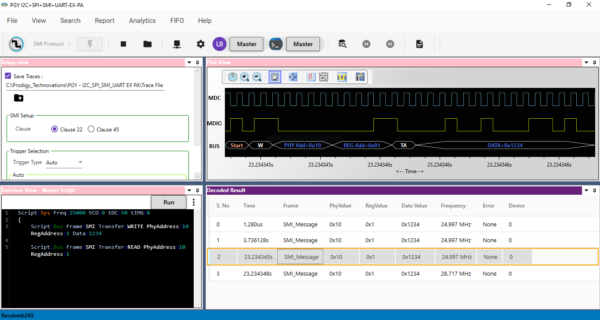
Figure 5: MDIO Protocol Analysis for clause 22 using PGY-MDIO-EX-PD
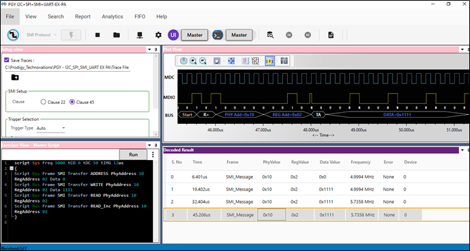
PGY-MDIO-EX-PD can generate traffic by adding a master or a slave device and then helps in decoding the packets with error injection capability. Users can easily select the clause with the help of a Graphical User Interface (GUI). PGY-MDIO-EX-PD provides an option to generate traffic through predefined scripts. The user can also configure the PHYADDR and REGADDR.
Users can capture protocol activity at specific events and decode the transition between the master and the slave. The decoded results can be viewed in the timing diagram and Protocol listing window with autocorrelation. This comprehensive view of information makes it the industry’s best, offering an easy-to-use solution to debug the MDIO protocol activity.
Figure 6: MDIO Protocol Analysis for clause 45 using PGY-MDIO-EX-PD
The timing view provides the plot of MDC and MDIO signals with a bus diagram. Overlaying of Protocol bits on the digital timing waveform will help easy debugging of Protocol decoded data. Cursor and Zoom features will make it convenient to analyze Protocol in the timing diagram for any timing errors. The protocol window provides the decoded packet information in each state and all packet details with error info in the packet. Selected frames in Protocol listing window will be auto-correlated in the timing view to view the timing information of the packet.


