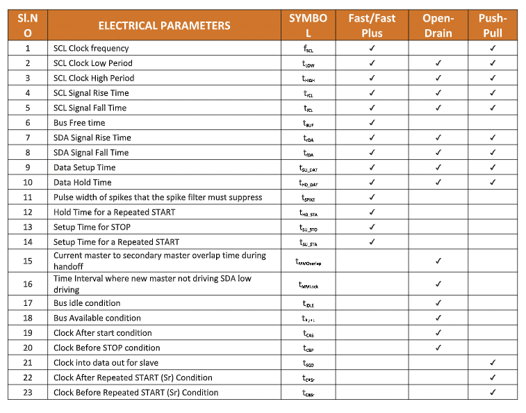
Introduction to MDIO:

Management Data Input/Output (MDIO), or Media Independent Interface Management (MIIM) is a serial bus protocol defined for the IEEE 802.3 standard Ethernet series of Media Independent Interface (MII). MII connects media access control (MAC) devices to Ethernet physical layer (PHY) circuits. The SMI/MDIO protocol is a simple two-wire serial interface that connects the management unit to the managed PHY to control the PHY and capture the status of the PHY. The Management Data Input/Output (MDIO) component can be used to read and write the PHY control register. Each PHY can be monitored before operation and the connection status can be monitored during operation. These registers provide status and control information such as link status, speed ability, and selection, power down for low power consumption, duplex mode (full or half), auto-negotiation, fault signaling, and loopback. The main purpose of using MDIO protocol is to configure the PHY layer transceiver parameters, for example, PHY devices can perform pre-emphasis or de-emphasis in the Physical Coding Sublayer (PCS), programming the control status registers in the PHY layer.

MDIO is a bidirectional shared bus structure that can provide a connection from the MAC (master) up to 32 PHY (slave) devices. All data is synchronously transmitted through the Management Data Clock (MDC), which is provided by the MAC and sent to all receiving devices. The data line is a tri-state shared bus that is MAC controlled for a write transaction or PHY controlled during a read transaction. The MDIO interface clock (MDC) supports frequencies up to 2.5MHz. The host processor, which is responsible for system configuration and monitoring, usually uses the MDIO host to perform individual access to various devices. MDIO was originally defined in Clause 22 of IEEE 802.3. To meet the growing needs of 10 Gigabit Ethernet devices, clause 45 of the 802.3ae specification is introduced.

MDIO System:

The MDIO bus has two signals: management data clock (MDC) and management data input/output (MDIO). MDIO has specific terms to define various devices on the bus. The device driving the MDIO bus is identified as a station management entity (STA). Target devices managed by MDC are called MDIO manageable devices (MMD). STA initiates all communications in MDIO and is responsible for controlling the clock on MDC. The specified frequency of MDC is up to 2.5 MHz. The following Figure captures the interface wiring diagram of a typical MDIO system.

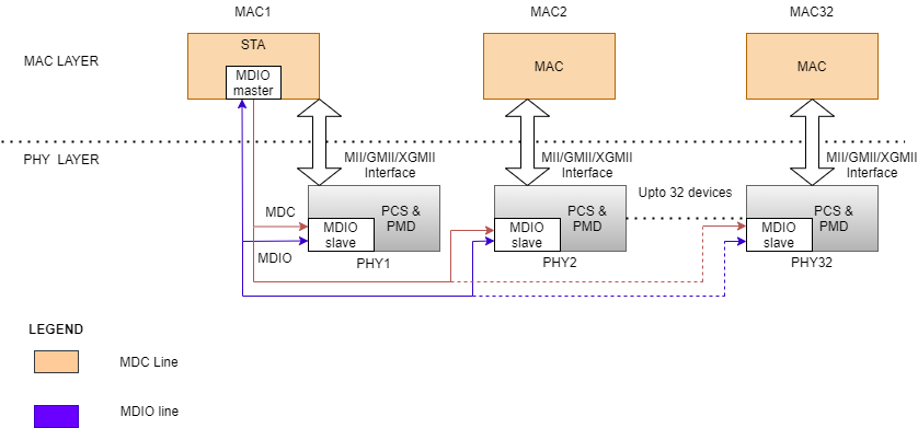
Figure 1: Wiring diagram of a typical MDIO Application.

MDIO (SMI Protocol) Features:

  • MDIO protocol has a configurable physical address.
  • MDC (clock bus) is specified to have a frequency of up to 2.5 MHz.
  • Capability added to address more registers–up to 65,536 registers in each device.
  • Variable MDIO speeds and duty cycle.
  • Power down for low power consumption.

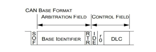
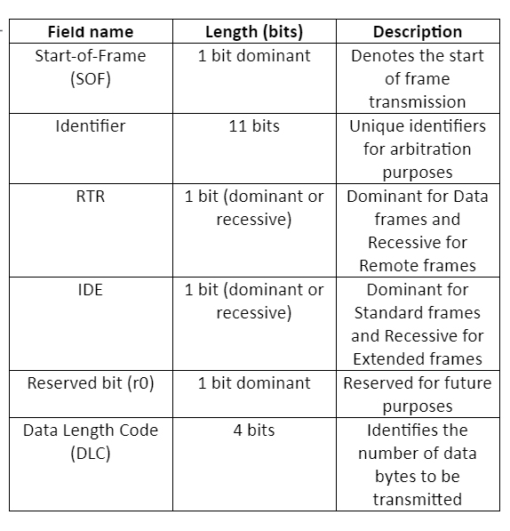
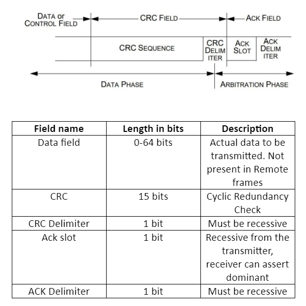
MDIO Protocol Frame Format:

CLAUSE 22:

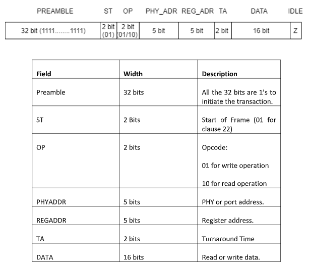
Figure 2: Clause 22 Frame format.

The MDIO data format for clause 22 is defined in the IEEE 802.3 Ethernet standard, as shown in the figure above.

Preamble (PRE): The first field in the MDIO protocol is indicated with Preamble. When the Preamble is sent, the MAC sends all bits as 1’s in the MDIO line. The 32 bits in the preamble are always 1’s.

Start (ST): The preamble is succeeded by the start bit which is 2 bits in size that remains 01 always in clause 22 for both read or write operations.

Opcode (OP): The next field is the opcode which gives information about whether a read or write operation is to be performed. Opcode with the value of ‘01’ in the frame specifies the write operation. Similarly, Opcode with the value of ‘10’ in the frame specifies read operation.

Physical Address (PHYAD): This field contains a 5-bit PHY address.

Register Address (REGAD): This field is 5 bits long indicating the register to be written or read from.

Turn Around (TA): The Turnaround field is 2 bits in size. When data is written to the PHY, the MAC will write “10” to the MDIO bus. When reading data, the MAC releases the MDIO bus.

Data: This field is 16-bit wide. During the read instruction, the PHY chip writes the data read from the REGAD register corresponding to the PHYAD in Data. During the write instruction, the MAC writes the value of the REGAD register corresponding to the PHYAD in Data.

Idle: At this state, MDIO is driven to a high impedance state, but it is generally pulled up with the help of a pull-up resistor.

CLAUSE 45:

Since there are not enough registers for future use, there was a need for Clause 45 to meet the growing need for 10-bit gigabit ethernet devices. There was little scope to cater multi the device’s PHY layer.

In addition, to read and write in Clause 22, additional commands are added in Clause 45. Clause 45 added support for low-voltage devices down to 1.2V and extended the frame format to provide access to many more devices and registers.

The MDIO data format for clause 45 is defined in the IEEE 802.3 Ethernet standard, as shown in the figure above.

The advantages of clause 45 over clause 22 are as follows:

  • Accessibility of 65,536 registers in 32 different devices across 32 different ports.
  • Additional OP and ST code for indirect access to register address for 10 Gigabit Ethernet.
  • Terminal fault signaling.  Multiple repeaters.
  • Low voltage specification

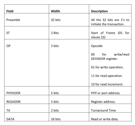
Figure 3: Clause 45 Frame Format

Preamble (PRE): The first field in the MDIO protocol is indicated with Preamble. When the Preamble is sent, the MAC sends all bits as 1’s in the MDIO line. The 32 bits in the preamble are always 1’s.

Start (ST): The preamble is succeeded by the start bit which is two bits in size that remain 00 always in clause 45 for all operations.

Opcode (OP): The next field is the opcode which gives information on whether a read or write operation is to be executed. Opcode with the value of ‘01’ in the frame specifies the write operation. The opcode with the value of 11 specifies the read operation. There exist additional two commands namely read increment and address. The read increment with opcode 10 does a read operation with the MMD device address incrementing after each access. The opcode with value 00 is to rewrite or reread DEV ADD’s address register.

Physical Address (PRTAD): This field consists of the 5-bit PHY address.

Device Address (REGAD): This field is 5 bits long indicating the registered address that must be written or read from.

Turn Around (TA): The Turnaround field is 2 bits in size. When data is written to the PHY, the MAC will write “10” to the MDIO line. When reading data, the MAC releases the MDIO bus to initiate driving read data if read operation.

Data: This field is 16-bit wide. During the read instruction, the PHY chip writes the data read from the REGAD register corresponding to the PHYAD in Data. During the write instruction, the MAC writes the value of the REGAD register corresponding to the PHYAD in Data.

Idle: At this state, the MDIO bus is driven to a high impedance state, but it is pulled up through a pull-up resistor of 1.5k ohm.

Theory of Operation:

The PHY devices require a preamble of 32 ones that must be sent by the MAC to PHY on the MDIO line. The register access consists of 16 control bits followed by 16 data bits. The control bits consist of 2 start bits, 2 bits for opcode or the type of operation (read or write), the PHY address (5 bits), the registered address (5 bits), and 2 turnaround bits. In a write instruction, the MAC provides the address and data. For a read instruction, the PHY receives from the MDIO stream during the turnaround, supplies the MAC with the requested register data, and then releases the MDIO stream.

When the MAC is driving the MDIO line, it must guarantee a steady value of 10 ns (setup time) before the rising edge of the MDC clock. In addition, the MDIO must remain stable for 10 ns (hold time) after the rising edge of the MDC. When the PHY drives the MDIO line, the PHY must provide an MDIO signal between 0 and 300 ns after the rising edge of the clock.

Therefore, with a minimum clock interval of 400 ns (max clock rate is 2.5 MHz), the MAC can safely sample the MDIO during the second half of the low clock cycle. The entire MDIO line is sampled on the rising edge of the clock except for the read operation. During the read operation, the MDIO line is sampled on the falling edge of the clock.

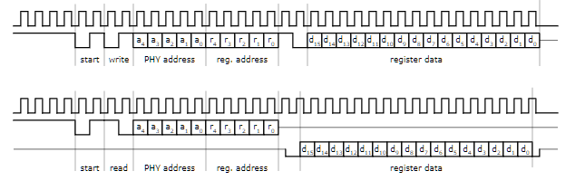
Figure 4: Theory of operation for clause 22.

Once the preamble is sent, the next two bits indicate the start operation. The start field is followed by a read or write operation. The corresponding PHY address is then sent on the MDIO line. The registered address of the PHY is then sent to the MDIO line. Both the addresses are 5 bits wide. During the turnaround, When the data is written to PHY, the MAC sends “10” indicating the line is free for the data to be written.

During the read operation, The MAC releases the MDIO line. The data is sampled during the read operation on the falling edge of the clock. If there is a mismatch with the PHY address, The value after the TA field will be continuously high. This means to say that MAC is trying to write to the register that does not exist.

Since there is a limit to using only 5-bit addresses for both PHYADDR and REGADDR, it limits the number of MMDs the STA can communicate with. Also, MDIO clause 22 only supports 5V tolerant devices and there is no low voltage option.

The main change in Clause 45 is how the registers are accessed. In Clause 22, both the address and read or write data are specified in one frame. Clause 45 changes this paradigm. First, an address frame indicating the MMD and the register is sent. Then a second read or write frame is sent.

An advantage of adding this two-cycle access is that clause 45 is backward compatible with clause 22, allowing the devices to communicate with each other. Second, by creating an address frame, the register address space is increased from 5 to 16 bits, which allows the STA to access 65,536 different registers. For this purpose, various changes have been made to the composition of the data frame. A new opcode (00) is defined to identify the data frames according to clause 45.

The OP codes have been extended to define an address frame, a write frame, a read frame, or an incremental read and post-read address frame. Since the registered address is no longer needed, this field is replaced with DEVADDR to indicate the type of target device. The extended device type allows the STA to access other devices in addition to the PHY.

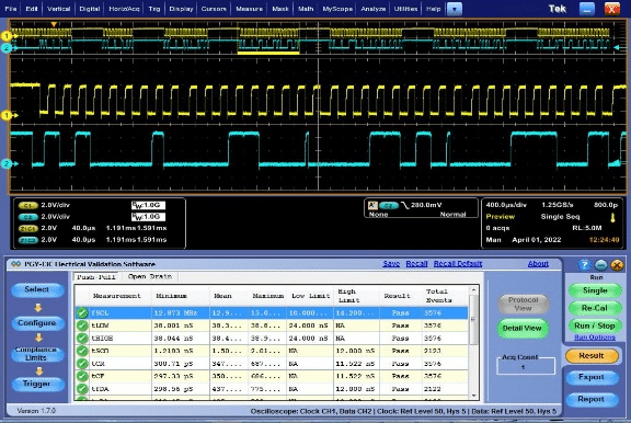
SMI/MDIO Protocol Challenges in Debug:

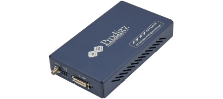
The MDIO Protocol Analyzer (PGY-MDIO-EX-PD) is a device that captures the data from the host and is designed under test. PGY-MDIO-EX-PD is a leading tool that enables the design and test engineers to evaluate the respective MDIO designs for their specifications by configuring the PGY-MDIO-EX-PD as a primary/secondary device, generating MDIO traffic and decoding the MDIO protocol decode packets.

MDIO Protocol Software

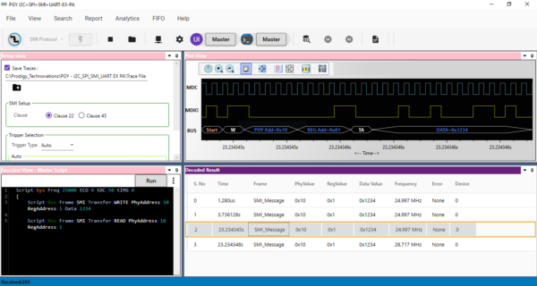
Figure 5: MDIO Protocol Analysis for clause 22 using PGY-MDIO-EX-PD

PGY-MDIO-EX-PD can generate traffic by adding a master or a slave device and then helps in decoding the packets with error injection capability. Users can easily select the clause with the help of a Graphical User Interface (GUI). PGY-MDIO-EX-PD provides an option to generate traffic through predefined scripts. The user can also configure the PHYADDR and REGADDR.

Users can capture protocol activity at specific events and decode the transition between the master and the slave. The decoded results can be viewed in the timing diagram and Protocol listing window with autocorrelation. This comprehensive view of information makes it the industry’s best, offering an easy-to-use solution to debug the MDIO protocol activity.

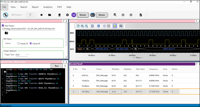
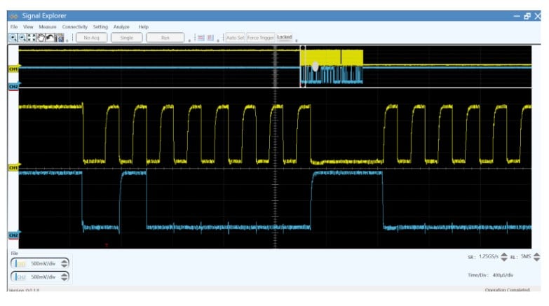
Figure 6: MDIO Protocol Analysis for clause 45 using PGY-MDIO-EX-PD

The timing view provides the plot of MDC and MDIO signals with a bus diagram. Overlaying of Protocol bits on the digital timing waveform will help easy debugging of Protocol decoded data. Cursor and Zoom features will make it convenient to analyze Protocol in the timing diagram for any timing errors. The protocol window provides the decoded packet information in each state and all packet details with error info in the packet. Selected frames in Protocol listing window will be auto-correlated in the timing view to view the timing information of the packet.

What is the role of the I3C Protocol in DDR5?

DDR5 has significant improvement over DDR4. DDR5 offers higher bandwidth with a data rate of up to 6.4 Gbps and operates at 1.1V consuming lower power compared to DDR4. The channel architecture is also significantly different compared to DDR4. DDR5 has two independent channels, unlike DDR4. To support additional performance and monitoring there are some interesting features as well.

Temperature Sensor IC on DIMM

DDR5 has two IC for temperature sensors TS1 and TS2. The purpose of these sensors is to monitor thermal changes in DIMM. Each of these DIMMs is strategically placed at the end of the DIMM to get the complete thermal profile of the DIMM. These temperature sensors use I3C interface Temperature sensors TS1 and TS2 can be controlled for fan speed changes and ensure the temperature profile is correctly maintained in the DIMM.

Image of DIMM with Temperature sensor.

Side Band Access:

DDR5 introduced a sideband bus to access non-DRAM modules. The Sideband bus is based on MIPI I3C or I3C Protocol. Apart from the sideband bus, there is also an SPD ie Serial Presence Detect Hub as the number of components has grown on DDR5. The SPD Hub interfaces the internal components of DIMM like RCD ie Register Clock Driver and PMIC and another temperature sensor IC.

Image of the Sideband bus

Debugging I3C Interface:

Prodigy has developed state of the art I3C Protocol analyzer. The I3C Protocol analyzer can be used to Debug the I3C Sideband bus in the DDR5 as well it can be used to check the protocol compliance of temperature sensors.

Prodigy I3C Protocol Analyzer

I3C devices are going through mass adoption at the moment. One challenge however remains for I3C devices is interoperability. The I3C devices need to work with devices of other manufacturers. Electrical validation of the physical pin level signaling plays a critical role in the Interoperability of the I3C Devices.

There are many parameters to the validated from an electrical validation perspective. However, some of the key parameters are listed below.

I3C Electrical Parameters table diagram

To capture I3C Signals for electrical validation, we need an oscilloscope with passive probes along with Prodigy PGY-I3C Electrical Validation and Protocol Decode Suite. The Oscilloscope and Probe bandwidth determines the measurement reliability.

The setup for the Electrical validation of I3C is as follows:

Hardware: Oscilloscope, this helps capture the signals required for electrical validation.

Software: The protocol validation suite measures the signal values and compares them with a specification to ensure compliance.

How to Setup the Hardware:

While selecting a scope, we must consider the minimum timing parameter that has a maximum impact on the oscilloscope bandwidth. In this case, the minimum timing parameter is 3ns rise/fall time. To measure this rise time, we need a scope with a bandwidth of 500MHz or more. Theoretically, the rise/fall time measurement capability of a 500MHz oscilloscope is 700ps. Considering the industry thumb rule, to measure a rise time of 3ns, we need at least 4 to 5 times the scope bandwidth. Hence 500MHz Analog bandwidth is recommended.

Oscilloscope Probe

However, the entire test setup bandwidth is dependent upon the oscilloscope and probe bandwidth. If we use lower bandwidth probes, then the RT/FT measurement capability is limited by the probe bandwidth instead of the oscilloscope. Hence, 1GHz passive probes with 2 to 3pf of capacitive loading are recommended so that the test setup is least intrusive.

Another important parameter to be considered for accurate measurement is the sample rate of the oscilloscope. For accurate measurement of rise and fall time, we need at least 5 to 6 samples on the rising or falling edge. Here, the signal is to be sampled at 500ps timing resolution. Hence, an oscilloscope with a sampling rate of 2GS/sec is recommended. Some of the oscilloscopes use efficient interpolation techniques and can provide better measurement even at around 1GS/sec

To make reliable measurements, it is advisable to capture the complete I3C frame in the acquisition memory of the oscilloscope. An oscilloscope with longer acquisition memory enables users to capture a greater number of I3C frames resulting in more instances of measurements. This increases measurement reliability and enables robust product design.

How to Run the Software:

The PGY-I3C Software runs inside Tektronix to make oscilloscopes such as MSO5/6, DPO/MSO5000, DPO7000, and DPO/DSA/MSO70000 series oscilloscopes. The PGY-I3C Electrical Validation and Protocol Decode automatically makes electrical measurements and provides protocol analysis with a long acquisition record length of up to 125MB that provides superior I3C Protocol Analysis results at the press of a button.

On July 28, 2022, congress passed the CHIPS and Science Act of 2022 to strengthen the domestic manufacturing of semiconductor chips in the U.S.

The $280 Billion CHIPS Act shall provide $52 Billion specifically to boost U.S. semiconductor manufacturing, development, and research. The $52 Billion package is divided into – 

  1. The $39 billion to companies building chip manufacturing plants in the U.S.
  2. The $11 billion to assist the chip manufacturing research and workforce training.
  3. The $2 billion to prompt lab innovation into the military and other applications.

The Act aims to compete with China and reduce U.S. dependency on South Korea and Taiwan for crucial semiconductor technologies. The U.S. share of global semiconductor manufacturing has declined from 37% in 1990 to only 12% in 2020. 

With these grants coming from the Chip Bill, the U.S. semiconductor companies like Micron have begun announcing a $40 billion investment in memory chip manufacturing. This has boosted the U.S. market share from 2% to 10%.

U.S. Chipmakers like Qualcomm, which specializes in mobile phone chips also agreed to acquire an extra $4.2 billion worth of semiconductor chips from Global Foundries’s New York manufacturing facility. 

Intel has committed to building a $20 billion chip plant near Columbus, Ohio. It has been estimated that 40,000 new job openings in the U.S. semiconductor market.

The Chip Act of 2022 doesn’t prevent U.S. chipmakers from producing outside the country but also doesn’t encourage the same. 

At present, there is a global chip shortage crisis affecting more than 169 industries. Global Chip buyers are desperate and would love the fresh chip supply from the U.S. but that’s a long road ahead. This is because building a chip plant is a long process, and new chip facilities require time for hiring talented and skilled staff.

Other factors like regulations, labor costs, and roadblocks common in U.S. manufacturing are likely to further slow down the process. As big as an achievement this is for the U.S. semiconductor market, the impact could take a decade to reflect. 

But the U.S. dominance in the global semiconductor market is inevitable. In the future, large U.S. corporations like Texas Instrument, and Intel shall take a huge market share. This will affect Asian companies, especially China. We would also see a huge manufacturing cost difference between Asia and the US.

Semiconductor characterization is one of the most complex activities to be carried out to offer very reliable solutions to end customers. Prodigy offers many versatile solutions for low and high-speed serial interfaces. Validation at the pre-silicon development level must be performed to find bugs in the design code. Our solutions can be used in emulation platforms, prototyping platforms, and later once the silicon is out of the foundry for post-silicon validation. These validations would involve running numerous functional test cases like generating protocol-specific traffic and injecting to the device under test during the emulation and at the prototyping time frame. During the post-silicon validation, you may like to vary some of the protocol packet content for error injection, the timing parameters of the signals, the amplitude variation, and the complete automation of the test environment. Prodigy provides a comprehensive solution to address all these needs. Our solutions include UFS4.0, PCI Express, I3C, SPMI, UART, JTAG, QSPI, etc. 

Read more about our products.

Introduction: I2C Protocol

I2C Protocol stands for Inter Integrated-Circuit. I2C is a simple two-wire design, half-duplex serial communication protocol, and the data is transmitted bit by bit over a single wire. I2C supports multiple masters and slaves on the bus, but only one master can be active at a time. Any I2C device can be attached to the bus allowing any master device to exchange information with a slave device. A device can operate either as a transmitter or a receiver depending on its function. Initially, I2C only used 7-bit addressing but evolved to allow 10-bit addressing as well. Three bitrates are supported: 100 kb/s (standard mode), 400 kb/s (fast mode) and 3.4 Mb/s (high-speed mode).

I2C Frame format:

  • Start indicates the start of operation and the device taking control that a message will follow.
  • ddress is a 7-bit/10-bit number representing the address of the device that will either be read from or written to.
  • R/W bit is a bit indicating whether the data will be read from or written to the device.
  • ACK is a bit from the slave device acknowledging the master’s action.
  • Data is an integer number of bytes read from or written to the device.
  • Stop indicates the message is complete and the master has released the bus.

Frame format - I2C Clock Stretching

Figure 1: I2C Frame Format

I2C Protocol: Theory of Operation:

I2C’s physical two-wire interface consists of bi-directional serial clock (SCL) and data (SDA) lines. Both SCL and SDA lines must be connected to Vcc through a pullup resistor. Data transfer is initiated only when the bus is idle. A bus is considered idle if both SDA and SCL lines are high after a stop condition.

I2C communication on the bus is initiated by the master sending a START condition and terminated by the master sending a STOP condition. A high-to-low transition on the SDA line while the SCL is high defines a START condition. A low-to-high transition on the SDA line while the SCL is high defines a STOP condition.

Repeated START condition is useful when the master wishes to start a new communication but does not wish to let the bus go idle with a STOP condition. Sending a stop condition can cause the master to lose control of the bus to another master (in multi-master environments). Hence, a repeated start condition is used. Here, instead of sending the STOP condition, the master sends another START condition followed by the address, read/write bit, and data. For generating a repeated START, the master changes the SDA line from high to low while the SCL line is high. In case the I2C bus remains busy, the master sets the SDA line to high during the low phase of the SCL to prepare for the repeated START condition.

One data bit is transferred during each clock pulse of the SCL. One byte consists of eight bits on the SDA line. A byte may either be a device address, register address, or data written to or read from a slave. Data is transferred the most significant bit (MSB) first. Any number of data bytes can be transferred from the master to the slave between the START and STOP conditions. Data on the SDA line must remain stable during the high phase of the clock period, as changes in the data line when the SCL is high are interpreted as control commands (START or STOP).

Each byte of data including the address byte is followed by one ACK bit from the receiver. The ACK bit allows the receiver to communicate with the transmitter that the byte was successfully received, and another byte may be sent. Before the receiver can send an ACK, the transmitter must release the SDA line. For all data bits, including the acknowledge bit, the master must generate clock pulses. If the slave device does not acknowledge the transfer, this means that there is no more data, or the device is not ready for the assignment yet.

The 9th clock cycle of SCL is for the ACK and NACK. The acknowledge signal is valid when the transmitter releases the SDA line during the acknowledge clock pulse. If the receiver pulls the SDA line low, and it remains at a stable low during the high period of the clock pulse, it indicates ACK. If the SDA line is drawn to high, then that signifies NACK.

Data must be sent and received to or from the slave devices, but the way in which it is accomplished is by reading or writing to or from registers in the slave device.

I2C Clock Stretching

Figure 2: Data Transfer on the I2C bus

Clock Stretching in I2C Protocol: 

An I2C master controls the clock speed and provides SCL on the line. It is possible for the slave device to “stretch” or hold the clock and alt the data or commands transmission from the master. Clock stretching is mainly used to hold the master device when the slave device is swamped. An I2C slave device can use clock stretching to push the master device into a wait state. When a slave device requires longer time to manage data, such as store received data or prepare to transmit another byte of data, it may execute clock stretching. This usually happens after the slave device has acknowledged receiving a byte of data.

I2C Clock Stretching

Figure 3: Illustration of Clock stretching in I2C

The clock stretching pauses the transaction by holding the SCL line LOW. The data transaction cannot be completed until SCL line held HIGH. Clock stretching is optional and in fact, most target devices do not include an SCL driver, so they are unable to stretch the clock.

A device may be able to receive bytes of data quickly at the byte level, but it takes longer to store a received byte or prepare another byte for transmission. After receiving and acknowledging a byte, targets can keep the SCL line LOW to force the controller into a wait state until the target is ready for the next byte transfer, like a handshake operation.

 A device, such as a microcontroller with or without limited I2C-bus hardware, can slow down the bus clock by lengthening each clock LOW period on the bit level. Any controller’s speed is adjusted to the device’s internal operating rate.

Clock Stretching using PGY_I2C_EX_PD:

Prodigy offers an I2C Protocol analyzer to capture and decode the I2C packets. I2C protocol analyzer has the advanced capability not only to trigger but long allow very long captures which is very useful for the embedded design engineer during the debug.

Capture of I2C Clock Stretching

Figure 4: Capture of I2C Clock Stretching

PGY_I2C_EX_PD Script - I2C Clock Stretching

Figure 5:PGY_I2C_EX_PD Script

PGY_I2C_EX_PD supports I2C clock stretching in both master and slave devices in Open Drain Mode only. In the above figure, the line in yellow signifies the SCL clock and the line in blue is Data line (SDA). The SCL clock is running at 400KHz. On the 9th clock of every I2C data transfer, the I2C slave pushes the SCL line low (before the ACK stage). The length of a clock stretching period is not limited by the I2C protocol.  As the SCL line remains LOW for a certain amount of time, the SDA line is held HIGH. I2C clock stretching can be enabled using the script shown below in PGY_I2C_EX_PD.

ABOUT THE AUTHOR

Deon Fleming Dsouza is a FPGA design engineer at Prodigy Technovations. He graduated from NMAM Institute of technology with a bachelor’s degree in Electronics and Communication Engineering. His areas of interest includes Digital System Design, VLSI circuit design, Computer communication and networking.

SMBus Protocol Introduction:

The System Management Bus (SMBus) is a two-wire interface through which various system component chips and devices can communicate with each other and with the rest of the system. It is based on the principles of operation of the I2C bus. SMBus provides a control bus for system and power management-related tasks.

SMBus is commonly used in personal computers for smart batteries, temperature control, and other low bandwidth system management communication. The original purpose of the SMBus was to define the communication link between an intelligent battery, a charger for the battery, and a microcontroller that communicates with the rest of the system. However, SMBus can also be used to connect a wide variety of devices including power-related devices, system sensors, inventory EEPROMs, communications devices, and more.

SMBus technology is used in Smart Battery Systems, or SBS, which is often implemented in portable devices such as laptop computers, mobile devices, and cameras for efficient battery management. Smart Battery Systems consist of a host, smart charger, and smart battery and use SMBus for these components to communicate with each other and the rest of the system. Smart Battery Systems are often beneficial to the battery life in portable devices. By using SBS, the battery can inform the charger about multiple aspects, including its capacity, ideal charging current, maximum charging time, and much more. Plus, because there is more precision with these variables, a Smart Battery doesn’t require recharging as frequently.

SMBus Master-Slave

SMBus vs I2C:

  • I2C defines input voltage levels as percentages of VCC, while SMBus operates with fixed input voltage levels. The I²C and SMBus specifications also specify the logic input threshold voltages, VIL and VIH, differently. The I²C specification requires that VIL be 30% of VDD and that VIH be 70% of VDD. The SMBus V3.0 specification has fixed thresholds. VIL is set to 0.8 V and VIH is set to 1.35 V.
  • SMBus requires a minimum bus clock frequency of 10 kHz (Except when the bus is idle). I2C has no such requirement. The maximum frequency of SMBus is 100 kHz, which equals the maximum speed of I2C operating in standard mode.
  • In I²C bus specification, the master may hold the clock line low forever and that would be a valid condition. In addition, the I²C specification permits a slave device to hold the clock line low for an unlimited amount of time. The SMBus specification places limits on the maximum amount of time a master may extend the clock low time within each byte of a message. There is also a limit on the total time a slave device may extend the clock low time within each message.
  • The I²C specifications do not require that a device always acknowledge its address. This can confuse a system controller whether it is because the device is busy, has failed, or has been removed. To prevent this confusion, the SMBus specifications require that an SMBus device always acknowledge its address. If a device that did acknowledge its address fails to do so the system controller, then knows that the device has either failed or has been removed.
  • For applications where power usage must be minimized, such as in battery-operated systems, the SMBus specification has a Low Power class. I²C does not have a similar specification.

SMBus Protocol Frame Format: 

Two unique bus situations define a message START and STOP condition.

START and STOP conditions

  1. A HIGH to LOW transition of the SMBDAT line, while SMBCLK is HIGH, indicates a message START condition. 
  2. A LOW to HIGH transition of the SMBDAT line while SMBCLK is HIGH defines a message STOP condition. START and STOP conditions are always generated by the bus master. After a START condition, the bus is busy. The bus becomes idle again after a certain time following a STOP condition. 

After the START condition (“S”), the master places the 7-bit address of the slave device it wants to address on the bus. The address is 7 bits long followed by an eighth bit indicating the direction of the data transfer (R/W#); a ZERO indicates a transmission (WRITE) while a ONE indicates a request for data (READ). A data transfer is always terminated by a STOP (P) condition generated by the master.

Every byte consists of 8 bits. Each byte transferred on the bus must be followed by an acknowledge bit. Bytes are transferred with the most significant bit (MSB) first.

Start and Stop Conditions

The acknowledge-related clock pulse is generated by the master. The transmitter, master, or slave releases the SMBDAT line (HIGH) during the acknowledged clock cycle. To acknowledge a byte, the receiver must pull the SMBDAT line LOW during the HIGH period of the clock pulse. A receiver that wishes to NACK a byte must let the SMBDAT line remain HIGH during the acknowledged clock pulse. An SMBus device must always acknowledge (ACK) its address. SMBus uses this signaling to detect the presence of detachable devices on the bus. An SMBus slave device may decide to NACK a byte other than the address byte in the following situations: 

  • The slave device is busy performing a real-time task, or the data requested are not available. The master upon detection of the NACK condition must generate a STOP condition to abort the transfer. Note that as an alternative, the slave device can extend the clock LOW period within the limits of this specification to complete its tasks and continue the transfer. 
  • The slave device detects an invalid command or invalid data. In this case, the slave device must NACK the received byte. The master upon detection of this condition must generate a STOP condition and retry the transaction. 
  • If a master receiver is involved in the transaction it must signal the end of data to the slave transmitter by generating a NACK on the last byte that was clocked out by the slave. The slave transmitter must release the data line to allow the master to generate a STOP condition. 

SMBus Protocol Theory of Operation:

The SMBus specification refers to three types of devices: host, master, and slave.

  • A host is a specialized master that provides the main interface to the system’s CPU.
  • A master is a device that issues commands, generates the clocks, and terminates the transfer.
  • A slave is a device that receives or responds to a command.

Each device that exists as a slave on the SMBus has one unique seven-bit address called the slave address. Each address is seven bits long with a read/write bit appended in bit position 0. When a device “sees” its address, it wakes up and responds to the rest of the command. Besides the General Call Address, SMBus systems can have 127 devices.

SMBus Protocol Theory of Operation Table

A typical SMBus device will have a set of commands by which data can be read and written. All commands are one byte long while their arguments and return values can vary in length. Accessing a command that does not exist or is not supported may cause an error condition. By the SMBus specification, the most significant bit (MSB) is transferred first. 

All the commands first put a start condition on the bus, then begin the transmission by transmitting the command/data, wait for an acknowledgment from the slave (receiving) device during command/data transmission, and then put a stop condition on the bus.

Following is a description of some basic SMBus command protocols:

Quick command—The R/W bit in the slave address denotes the commands. An example of using it is to turn it on/off or to enable/disable a device function. There is no data sent or received.

SMBus Protocol Theory of Operation

Send byte—The data byte sent contains the features to be accessed and actions for this feature to execute.

Slave address 2

Receive byteThe Receive byte is like a Send byte; the only difference is the direction of data transfer. The Receive byte is used when the host accesses the device for some information.

Packet Error Checking 

The Packet Error Checking mechanism improves reliability and communication robustness. Packet Error Checking, whenever applicable, is implemented by appending a Packet Error Code (PEC) at the end of each message transfer. Each protocol (except for Quick Command and the host notify protocol) has two variants: one with the Packet Error Code (PEC) byte and one without. The PEC is a CRC-8 error-checking byte, calculated on all the message bytes (including addresses and read/write bits). The PEC is appended to the message by the device that supplied the last data byte.

Synchronization

A situation may occur in which more than one master is trying to place clock signals on the bus at the same time. The resulting bus signal will be the wired-AND of all the clock signals provided by the masters. A high-to-low transition on the SMBCLK line will cause all devices involved to start counting off their LOW period and start driving SMBCLK low if the device is a master. As soon as a device finishes counting its LOW period it will release the SMBCLK line. Nevertheless, the actual signal on the SMBCLK may not transition to the HIGH state if another master with a longer LOW period keeps the SMBCLK line LOW. In this situation, the master that released the SMBCLK line will enter the SMBCLK HIGH wait period. When all devices have counted off their LOW period, the SMBCLK line will be released and go HIGH. All devices concerned at this point will start counting their HIGH periods. The first device that completes its HIGH period count will pull the SMBCLK line LOW and the cycle will start again.

Synchronization

Arbitration

A master may start a transfer only if the bus is idle. One or more devices may generate a START condition within the minimum hold time resulting in a defined START condition on the bus. 

Since the devices that generated the START condition may not be aware that other masters are contending for the bus, arbitration takes place on the SMBDAT line while the SMBCLK is HIGH. A master that transmits a HIGH level, while another master (or masters) is transmitting a LOW level on the SMBDAT line loses control of the bus in the arbitration cycle.

This mechanism requires that SMBus master devices participating in an arbitration cycle monitor the actual state of the SMBDAT line during the arbitration.

ABOUT THE AUTHOR

Anuj is an FPGA Design Engineer at Prodigy Technovations. He graduated from NMAM Institute of Technology with a bachelor’s degree in Electronics and Communication Engineering. He has hands-on experience in debugging and fixing hardware issues reported during product development and has rich experience in resolving customer issues during product evaluation.

Prodigy’s SMBus Protocol Exerciser and Analyzer

SM Bus Serial bus interface has been widely used for voltage and temperature monitoring of the system. PGY-SMBus-EX-PD is the leading instrument that enables the design and test engineers to test the SM Bus designs for its specifications by configuring PGY-SM Bus -EX-PD as master/slave, generating SM Bus traffic with error injection capability and decoding SM bus Protocol decode packets.

Today’s automobiles are not just about engines and wheels, it is much more. The factor that defines these automobiles is the electronic functionality with advanced technologies and safety features embedded in them. These electronic functions are controlled by Engine Control Units (ECUs), Transmission Control Units (TCUs), and Body Controlled Module (BCM). These control units need to be interconnected and they must communicate with each other. To establish this communication, there are several protocols, out of which the Local Interconnect Network (LIN), Controller Area Network (CAN), and FlexRay are predominantly used. Each of these protocols is used for different applications depending upon their behavior and characteristics.

Now, let us look at the brief introduction of these protocols.

LIN Protocol:  LIN stands for Local Interconnect Network; it is a serial communication and low-cost protocol for various low-speed and non-critical electronic applications in an automobile. It is a master-slave type of communication-based on a polling strategy (like UART) and it is half-duplex or one-way communication at a given time. There is 1 Master and up to 15 slaves on a LIN bus. The communication between the Master and Slaves happens through a fixed frame structure initiated by the master always. The slave/(s) respond to the header accordingly. It is important to note that, sometimes the master can respond to its header.

CAN Protocol: CAN stands for Controller Area Network, which is a serial communication protocol supporting distributed real-time control with a very high level of security and efficiency. It is a broadcast type of protocol, in which the concept of ‘Master’ and ‘Slave’ is not present. The communication between nodes happens in a fixed frame structure. Any device/node having an update over a specific activity from any application could transmit the corresponding frame and every other device/node on the bus could read this frame and respond to it correspondingly. During such a situation, conflict on the bus is inevitable. This is resolved by ‘bit-wise arbitration’.

FlexRay Protocol: FlexRay is a fault-tolerant, deterministic, and high-speed automotive networking serial communication protocol. The fundamental idea of designing the FlexRay protocol was to meet the high-speed requirements of various applications in an automobile. Even in this protocol, multiple nodes are trying to communicate and there is no master-slave concept present. Each node is given a specific time during which the communication happens. A fixed frame structure is used to communicate between the nodes.

Now, let us look at the similarities and differences between these three protocols.

Parameters LIN CAN FlexRay
Architecture Single master and up to 15 slaves Multiple nodes (20, 32) Multiple nodes (up to 64)
Medium access or Bus access Polling method CSMA-CR method TDMA method
Topology Bus topology Bus topology Bus/Star topology
Message transmission Synchronous Asynchronous Synchronous/Asynchronous
Data rate or Baud rate Max. 20kbps Max. 1Mbps Max. 10Mbps
Bit coding NRZ NRZ and bit stuffing NRZ
Error checking mechanism Checksum over the Protected Identifier and Data fields CRC computation over the entire frame Two CRC computations.

1. Header CRC: Over the header field (starting from the Sync frame indicator field)

2. Trailer CRC: Over the entire frame

Hamming Distance (HD) HD for the checksum is 2 HD for the CRC computation is 6 HD for the header CRC is 6 and for the trailer CRC it is 6 up to 2048 bits and 4 for data up to 4096 bits.
Physical layer Single electrical wire Electrical dual wire Dual wire – optical or electrical operating
Operating voltage 8v to 9v 3.3v Differential voltage of +2.0v
Cabling impedance 1k ohms 120 ohms 80-110 ohms
Range 1-5 kilometers 40 meters 10 meters

After getting an idea about the differences, now let us look at their pros and cons.

Advantages of LIN protocol:

  • As LIN is a single wire-based interface, it reduces the cost and the complexity of implementation. 
  • LIN is self-synchronized and therefore no need for external oscillators.
  • LIN is the best and the most suited alternative to the CAN for applications that do not need high bandwidth and that are of low speed.

Disadvantages of LIN protocol:

  • Since LIN is a low speed, it is not considered for safety and other important applications.
  • The communication is always initiated by the master and therefore when the master device fails then the whole bus gets failed.
  • There are no strong error-checking mechanisms in LIN.

Advantages of CAN protocol:

  • CAN is used in different electrical environments which offers noise-free transmission.
  • In CAN any node on the bus can initiate the communication and any node can respond. Therefore, the failure of one device/node will not lead to the failure of the entire system.
  • CAN protocol offers strong error-checking mechanisms.

Disadvantages of CAN protocol:

  • CAN bus is more expensive than the LIN
  • Implementing CAN is a bit more complex than that of LIN due to the increased number of nodes.

Advantages of FlexRay:

  • FlexRay is a deterministic, fault-tolerant, and high-speed protocol than that CAN protocol and therefore FlexRay is mostly used in safety-critical applications.
  • Since FlexRay is a synchronous protocol, it synchronizes its nodes without an external synchronous clock.
  • The star topology of the FlexRay reduces the exposed wire for the segment which in turn decreases the noise.
  • It has a better error-checking mechanism compared to LIN and CAN.

Disadvantages of FlexRay:

  • It is expensive compared to LIN and CAN protocols.
  • It is a bit complex to implement
  • It has lower operating voltages

Now, let us look at the applications of these protocols.

Applications of LIN

LIN is used in non-critical applications like:

  • Sunroof sensors
  • Light sensors
  • Wiper sensors
  • Climate control sensors
  • In engines for engine fan cooling sensors

Applications of CAN

  • CAN is used as a controller which makes direct communication with Engine Control Units (ECUs) for applications that are used by LIN.
  • CAN also find its application outside the automotive industry such as in Avionics, Industrial automation, and escalators and elevators.
  • CAN is used for internal hardware communication of a control unit or a CPU inside Battery Management Systems (BMS).

Applications of FlexRay

FlexRay is used in safety-critical applications like:

  • Power train module
  • Safety suspension
  • Adaptive Cruise Control

Finally, to summarize, it all depends on the application requirements to choose between these three protocols. Despite their cons, all three of them serve their purpose to their best for a given application. Therefore, these protocols are widely used in automotive applications and other industrial applications even to this date.

ABOUT THE AUTHOR

Sumukha Bharadwaj is an FPGA Design Engineer at Prodigy Technovations. He has a Master’s Degree in Engineering – Information Technology from SRH Hochschule Heidelberg University, Heidelberg, Germany. His area of interest includes Digital Systems Design, Avionics, Automotive Electronics, and Embedded Systems.

What is CAN protocol?

The Controller Area Network (CAN) is a serial communications protocol that supports distributed real-time control with a very high level of security and efficiency. 

Where is CAN Protocol Used?

CAN is extensively used (but not restricted) in the automotive industry for automotive electronics precisely in the engine control units (ECUs), for various applications involving sensors, anti-skid systems, etc. The numerous ECU functions used in an automotive vehicle are managed by microcontrollers. To establish communication between the microcontrollers and devices with each other’s applications without needing a host computer, a bus architecture known as CAN is robustly designed. 

How does CAN communicate?

CAN is a message-based protocol and for each device, the data in a frame is transmitted sequentially. The message onto the bus is transmitted serially using a Non-Return-to-Zero (NRZ) format. 

CAN Protocol: Theory of Operations

Bit rate: The bit rate of a CAN bus in a given system is uniform and ranges up to a maximum of 1 Mbps (excluding CAN-FD). CAN-FD could have a variable bit rate in a given system and ranges up to a maximum of 5-8 Mbps.

Broadcast: CAN is a broadcasting type of communications protocol, in which the concept of ‘Master’ and ‘Slave’ is not present. Any device having an update over a specific activity from any application could transmit the corresponding frame and every other device on the bus could read this frame.

Arbitration: Since CAN is a broadcasting type of communication protocol, multiple devices tend to communicate at the same time. During such a condition, conflict on the bus is inevitable. To solve this type of problem, bitwise arbitration is adopted. Whichever device wins the arbitration, gets to communicate and others back off.

Error Detection: All CAN nodes are implemented with powerful measures for error detection, signaling, and self-checking, and these measures are:

  • Monitoring (the bit levels of the data to be transmitted will be continuously compared by the transmitter with the bit levels detected on the bus).
  • Cyclic Redundancy Check (CRC) – CRC is adopted to ensure that the data in the frame is received flawlessly.
  • Bit stuffing – After every 5 consecutive homogeneous bits a bit with an opposite polarity is introduced. This is called bit stuffing.

Now let’s get into the CAN frame formats and the way they look.

CAN Frames Format :

The message transfer is done through four types of frames, and they are: 

Data frames: Carries the data between transmitter and receiver

Remote frames: A bus unit can request the transmission of a data frame with the same Identifier by sending this remote frame to the transmitter.

Error frames: When a bus error is detected, an error frame is transmitted.

Overload frames: An overload frame is transmitted to provide an extra delay between frames (a standard amount of delay is provided by Interframe space) during multiple frames transmission.

Each Data frame and Remote frame has two different types of frame formats, and they are, Standard frame and Extended frame.

Alright, pictures speak more than words! Let us show the frames


These fields are the same for both Data and Remote frames. The next fields are shown in the below figure.

After all these fields, it is the End-of-Frame field which consists of seven consecutive 1’s, indicating the end of transmission.

Seven consecutive 1’s? What about bit stuffing then?

Well, bit stuffing is done only till the CRC-Delimiter field. The remaining fields are fixed in a frame. Hence, no bit stuffing is done to the Acknowledgement field and End of frame field.

Okay, now what’s the difference between the Standard frame and the Extended frame? As well as between the Data frame and Remote frame?

One at a time; The only difference between Standard and Extended frames is that the identifier is of 29-bits in Extended frames whereas, 11-bits in Standard frame formats. The 29-bits are categorized into two ID fields, first, 11-bits are as same as in the Standard frame and next 18-bits in another field. The below figure shows the difference between the two frames.

The SRR field is Substitute Remote Request, and it is transmitted as recessive.

Well, now with the Data frame and Remote frame. A data frame is shown in the above figure. The remote frame is the same as the Data frame except that the Data field is not present. So, it comprises of SOF, Arbitration field, Control field, CRC field, ACK field, and EOF. 

Great! Next, what’s with that CAN-FD?

CAN-FD stands for CAN Flexible Data Rate. This was introduced to increase the bandwidth on the bus by increasing the bit rate. Meaning, the bit rate on a given system during the frame transmission could change to a higher speed.

Oh, that’s nice! What about the frame structure?

CAN-FD has a similar frame structure to that of normal CAN, and two different types of frame formats as that of normal CAN, standard and extended frames, but there are no Data frame and Remote frame concepts here. The below figure gives a clear idea about the same.

The only fields that are different from normal CAN are, EDL, BRS, and ESI

The CAN FD extended frame format consists of a 29-bit identifier and an SRR field which is recessive one bit. And the rest of the fields remain the same as that of the CAN FD standard frame format.

CAN Protocol Challenges in Debug

Well, the challenges during the debug are:

  1. Identifying different types of errors on the CAN bus
  2. Capture time for long data bytes and error checking for the same

Debugging CAN Protocol

To Debug CAN Protocol we need a very good protocol analyzer. Prodigy’s CAN Protocol Analyzer is capable of decoding every field in the frame and providing the user with the necessary information related to timing and data. The user can see this piece of information through the software UI.

The user can also set triggers for different conditions through the software GUI. The analyzer is then capable of triggering all the error conditions on the bus as well as at different fields in the CAN frame as set by the user. The analyzer constantly analyzes the bus for any errors and if found any, it reports, and this can be seen in the software UI.

The analyzer also checks for the CRC on the bus. Meaning, it receives the frame from the CAN Transmitter, decodes it, and calculates the CRC at its end. It displays the calculated CRC and the received CRC and throws an error if the comparison does not match. All this information can be viewed in the software UI.

The software is working in tandem with the hardware (Protocol Analyzer) and thus, the settings made through the GUI will be updated to the hardware and the analyzer then works accordingly.

Learn more about CAN Protocol Analyzer

About the Author :

Sumukha Bharadwaj is an FPGA Design Engineer at Prodigy Technovations. He graduated from the K S School of Engineering and Management in 2015 with a Bachelor’s degree in Electronics & Communication Engineering. He also completed his Master of Engineering, Information Technology from SRH Hochschule Heidelberg.

About Prodigy Technovations :

Prodigy has developed state of the art Protocol analyzer to debug various Protocols. The protocol analyzers range from CAN, I2C, SPI, QSPI, I3C, and UFS Plus many other protocols on the serial bus.

The automotive industry is going through a massive transformation. The consumer-based digital technologies and experiences are pushing the car in vehicle Information system to the next level. Consumers are asking for cars with mobile-like experiences. The Infotainment system needs to provide a touch-like experience and also support heavy workloads of storage map and navigation data as the car gets connected to the cloud.

How does the car OEM go ahead and select the memory for the next-generation Infotainment system?

How does the car OEM go ahead and select the memory for the next-generation Infotainment system?

What are the factors for selecting the automotive Infotainment memory solution?

Automotive Infotainment memory solution is selected based on the following factors 

  • Storage Capacity
  • Performance
  • Speed
  • Reliability
  • Faster Read and write cycles

Traditionally the memory had limited applications and one would go ahead with the Emmc Interface, however, the current emmC has run out of capacity when coming to advanced Infotainment system applications in the car.

What are the limitations of emmC when it comes to the Infotainment system?

  1. Emmc has a limited number of reads that are written like any other flash architecture and the memory begins to start to degrade. The automotive life span is over 10 plus years however memory card storage ie 8GB emmC would have a life of up to 4 years. Most advanced cars like Tesla earlier used 8GB storage and had to replace them with 64GB storage for the emmC ensuring longer life of the emmC.
  2. High Definition of media playback operations: The next generation of consumers is demanding new experiences like augmented reality and immersive experience. This is forcing car manufacturers to look at advanced technologies which can offer simultaneous read-write cycles. EMMC is half duplex ie it can either support the read or write cycle.
  3. Data Integrity: Emmc offers very limited support for data integrity such as write protection and error correction.

What is the path forward?

UFS seems to have very promising technology offering a good replacement solution for the Emmc when it comes to the Infotainment system. UFS is much faster and is already used in current-generation mobile to offer an immersive experience. UFS offers a full duplex interface for read and write increasing speed and giving high performance and also speeds up to 4800MB/s and vendors like Samsung have released memory chips supporting up to 1TB of data. UFS is engineered to support low-power mode which is extremely important for any automotive application. UFS also has advanced features like Error correction to have safe and reliable storage for automotive applications. We have to wait and see how the various memory vendors like Kioxia, Samsung, and Silicon Motion have their solutions for Automotive grade UFS. 

Prodigy Technovations offers state of art advanced tools to test UFS, emmC, and PCIe interfaces of the memory. The tools can help automotive car manufacturers debug protocol data and help find out very critical timing and protocol integrity issues.

Current Challenges in Automotive flash storage Technologies

The automotive industry is going through a mega transformation. The consumer-based digital technologies and experiences are taking over car vehicle Information systems. Consumers are asking for cars with mobile-like experiences pushing the car OEMs and manufacturers to look for next-generation In-vehicle entertainment display and storage solutions. The cars are getting connected to the cloud as well creating a need for storage on the edge of the car as well storage on the cloud. The need for faster high-performance memory is the need of the hour. The number of data in the current generation of cars is increasing to 4TB per day.

How does the car OEM go ahead and select the next-generation storage solution?

What are the factors for selecting the automotive storage solution?

The automotive storage solution is selected based on the following factors

  • Speed
  • Storage Capacity
  • Performance
  • Data Integrity
  • Reliability
  • Hi-speed Performance
  • Support Various kinds of Workloads- Read, Write, a mix of read and write.

The next-generation cars have various applications such as an Infotainment system, ADAS, and cloud connectivity. Each of these applications needs a different kind of memory with different interfaces and speeds.

Automotive Memory

The emmC is for the storage of maps and GPS navigation data. The UFS will need to support the Infotainment system with high-speed read cycles. The Cloud data will be stored in PCIe-based NVMe which will help in the machine learning and deep learning computations.

Challenges with current storage or memory systems in the car

Data Integrity and Reliability are one of the biggest concerns in the automotive system. There are regular power fluctuations causing data in the memory to get corrupted. Plus long storage cycle compared with frequent reads and writes can also reduce the life cycle of the flash device. To address the data integrity issues there is a need to build a system for error detection and error correction. Some of the memory vendors provide good solutions for detecting errors. Another challenge the automotive subsystem faces is the variation of temperature. The memory is subject to extreme variations in temperature during the lifecycle of the automobile.

Prodigy Technovations offers state of art advanced tools to test UFS, emmC, and PCIe interfaces of the memory. The tools can help automotive car manufacturers debug protocol data and help find out very critical timing and protocol integrity issues.

Request For Quote

Share your requirement and our team will provide a tailored quote based on your validation needs.

"*" indicates required fields

This field is for validation purposes and should be left unchanged.
Address*

Request For Demo

Tell us your use case and our team will schedule a product demo aligned to your validation workflow.

"*" indicates required fields

This field is for validation purposes and should be left unchanged.
Address*

Request A Demo

Tell us your use case and our team will schedule a product demo aligned to your validation workflow.

"*" indicates required fields

This field is for validation purposes and should be left unchanged.
This field is hidden when viewing the form
Address*

Request Quote

Share your requirement and our team will provide a tailored quote based on your validation needs.

"*" indicates required fields

This field is for validation purposes and should be left unchanged.
Address*