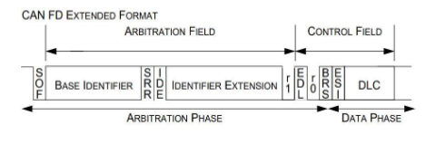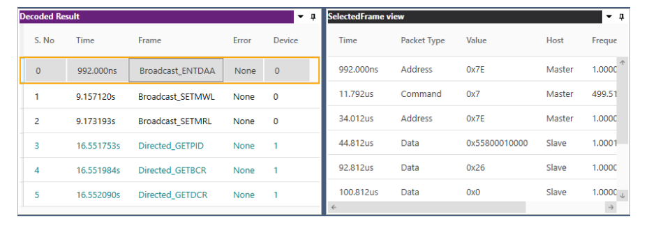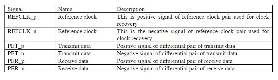
SPI Protocol: Introduction
SPI stands for Serial Peripheral Interface and it is a synchronous serial communication interface used for short-distance communication. SPI interface was developed by Motorola in the 1980s to be primarily used in embedded systems and since then it has become a de facto standard. SPI interface is widely used in SD cards, RFID card reader modules, and 2.4GHz wireless transmitters and receivers to communicate with microcontrollers.
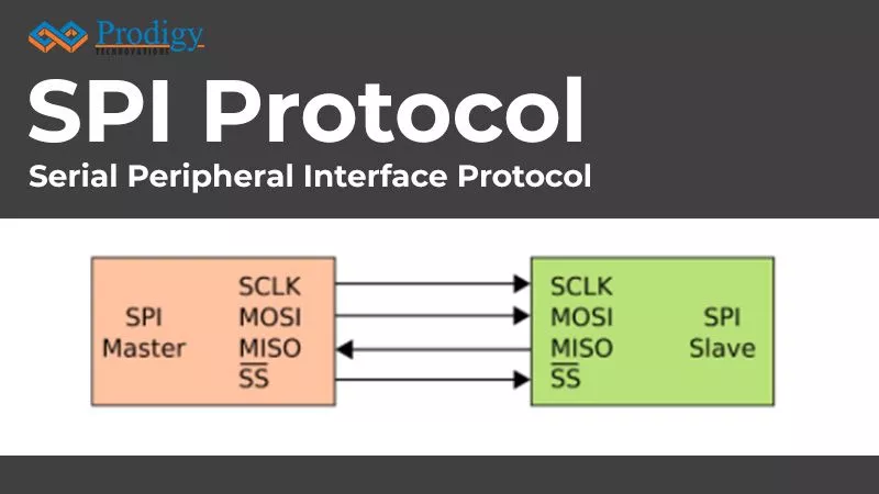
SPI is a full duplex protocol that uses a master-slave architecture with a single master. The master is the controlling device which is usually a microcontroller, while the slave is usually a sensor, display, or memory chip that takes instructions from the master. The simplest configuration of SPI is a single master-single slave system, but one master can control more than one slave. One unique benefit of SPI is that the data can be transferred without any interruption and any number of bits can be sent or received in a continuous stream.
Figure 1. Single Master to Single Slave SPI Interface
THE SPI INTERFACE
SPI requires four signals namely;
- Serial Clock (SCLK) – SCLK is a line for the clock signal.
- Master In Slave Out (MISO) – Line for slaves to send data to the master.
- Master Out Slave In (MOSI) – Line for master to send data to the slave.
- Slave Select (SS) – Line for the master to select which slave to send the data to.
Three signals are shared by all devices on the SPI bus: SCLK, MOSI, and MISO. SCLK is generated by the master and it is used for synchronization. MOSI and MISO are the data lines used for data transfer between master and slave. The direction of transfer can be both ways simultaneously, but an SPI device interested in only transmitting data can choose to ignore the receiving bytes and a device only interested in the incoming bytes can transmit dummy bytes. Each device has its own SS line. The master pulls low on a slave’s SS line to select that particular slave for communication.
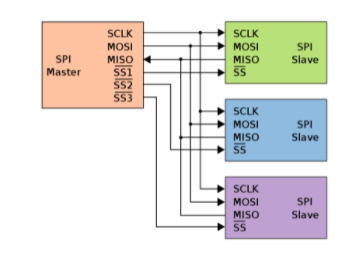
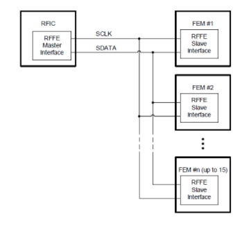
Figure 2. Typical SPI bus: One master and Three slaves
SPI Protocol: Theory of operations
THE CLOCK
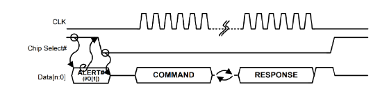
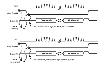
The clock signal synchronizes the output of data bits from the master to the sampling of bits by the slave. One bit of data is transferred in each clock cycle, so the speed of data transfer is determined by the frequency of the clock signal. SPI communication is always initiated by the master since the master configures and generates the clock. The clock signal in SPI can be modified using the clock polarity and clock phase. These two configurations work together to define when the bits are at the output when sampled. Clock polarity can be set by the master to allow for bits to be at the output and sampled either on the rising or falling edge of the clock cycle. The clock phase can be set for output and sampling to occur either on the first edge or the second edge of the clock cycle.
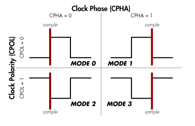
Figure 3. SPI Modes
SLAVE SELECT (SS)
The master can choose which slave he wants to talk to by setting the slave’s SS/CS line to a low voltage level. In the idle, non-transmitting state, the slave select line is kept at a high voltage level. Multiple SS/CS pins may be available on the master which allows for multiple slaves to be wired in parallel. If only one SS/CS pin is present, multiple slaves can be wired to the master by daisy chain configuration. The SPI bus can operate with a single master device and with one or more slave devices. If a single slave device is used then the SS pin may be fixed to logic low.
MOSI AND MISO
The master sends data to the slave bit by bit in serial using the MOSI line. The slave receives the data sent from the master at the MOSI pin. Data sent from the master to the slave is usually sent with the MSB first. The slave can also send data back to the master through the MISO line in serial. The data sent from the slave back to the master is usually sent with the LSB first.
DATA TRANSMISSION
To initialize the data transmission the master first outputs the clock signal. The master then switches the SS/CS pin to a low voltage level which activates a particular slave after which the master sends the data one bit at a time to the slave along the MOSI line. The slave reads the bits as they are received. If a response is needed, the slave returns the data one bit at a time to the master along the MISO line. The master reads the bits as they are received.
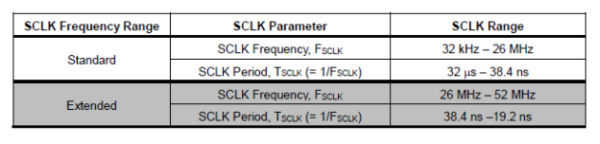
TRANSMISSION SPEED OF SPI PROTOCOL
The maximum SPI clock speed is dependent on the number of devices on the bus. There is no true maximum clock speed of SPI and it is solely dependent on the clock. SPI bus can run at high speeds transferring data at up to 60Mbps over short distances. SPI clock frequencies can reach up to 25MHz theoretically, but in practice, the maximum clock is limited to the frequency explicitly specified in the electrical specifications in the datasheet.
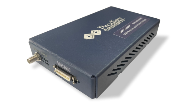
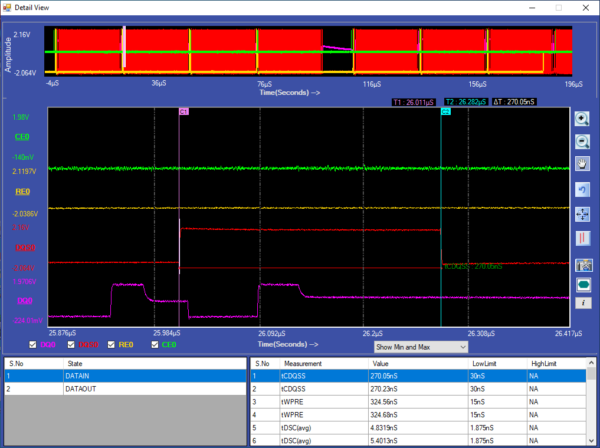
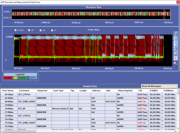
DEBUG OF SPI PROTOCOL
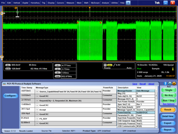
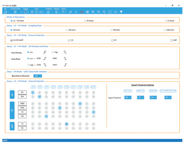
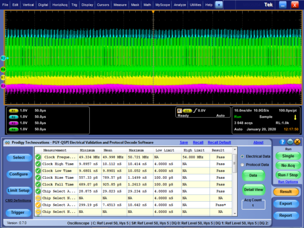
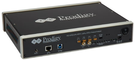
Debug of SPI Protocol can be easily done using a Protocol Analyzer. Prodigy Technovations has developed SPI Protocol Analyzer that can debug the SPI Protocol.
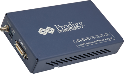
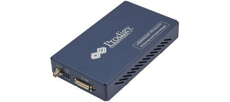
Prodigy’s SPI I2C Protocol Analyzer
About Prodigy:
Prodigy Technovations is the leading provider of protocol analysis solutions. Prodigy has developed state of the art Protocol analyzer to debug various Protocols. The protocol analyzers range from CAN, I2C, SPI, QSPI, I3C, PCIe, and UFS Plus many other protocols on the serial bus. Check out our products!