WHAT IS TRIGGERING?

The triggering feature allows engineers to capture a particular event of interest or data. Logic analyzers can be triggered on a variety of logical (Boolean) conditions. The purpose of the trigger is to select data to be captured by the logic analyzer. Logic analyzers can keep track of DUT logic states and trigger when a user-defined event occurs in the DUT. 

Many conditions can be set to trigger a logic analyzer. The most commonly used triggers include the Auto trigger, Pattern trigger, and Timing trigger. Using these trigger conditions, it is possible to track down system errors and then refine the search with increasingly explicit triggering conditions.

Prodigy Technovations Logic Analyzer supports four types of triggering. Auto, Pattern, Protocol awareness, and Timing parameters. Users can also trigger on any of the listed protocol packets. 

AUTO TRIGGER

In Auto Trigger mode, no trigger pattern is used and all data packets from the DUT are analyzed. Here, the acquisition is started as soon as the ‘Acquire‘ Button is clicked and the logic analyzer hardware starts capturing the activities in the DUT without waiting for any trigger event. 

PATTERN TRIGGER

Pattern trigger looks at a serial data stream and triggers after a given serial pattern is matched. 

The pattern trigger function allows the device to be configured to monitor the logic analyzer inputs for a specific pattern. When the logic analyzer comes across the specific pattern defined, the device is triggered.

Logic Analyzer Triggers

Figure 2. Pattern Trigger UI

Example: The Pattern is set as “0111001101” in binary as shown below and the logic analyzer triggered at that particular pattern indicated by the symbol “T”.

Logic Analyzer Triggers

Figure 3. Pattern Trigger Result 

PROTOCOL AWARE TRIGGER 

Protocol Aware trigger allows users to set trigger conditions on a set of listed protocols like I2C, SPI, UART, and their various parameters.

I2C PROTOCOL TRIGGER

I2C Protocol mode has various features to set trigger conditions on Start, Address, Data, Address+Data, Ack, Nack, Repeated Start, and Stop. Thus, giving engineers the flexibility to trigger on a particular set of listed parameters, which helps debug I2C design-related problems.

I2C bus debugging will be explained further in a detailed article. 

Logic Analyzer Triggers

Figure 4. I2C Trigger Menu 

SPI PROTOCOL TRIGGER

SPI protocol mode has features to set trigger conditions on MOSI data equal to/not equal to and MISO data equal to/not equal to a particular value that can be defined in Binary, Hex, Decimal, and Octal accordingly. 

Logic Analyzer Triggers

Figure 5. SPI Trigger Menu

UART PROTOCOL TRIGGER

UART protocol mode has various features to set trigger conditions on data equal to/not equal to a particular value that can be defined in Binary, Hex, Octal, and Decimal. The logic analyzer can also be set to trigger on either Odd parity or Even parity

Logic Analyzer Triggers

Figure 6. UART Trigger Menu

TIMING PARAMETER TRIGGER 

The timing parameter trigger allows users to set trigger conditions on pulse widths and delays of their choice. 

PULSE WIDTH TRIGGERING

The pulse width trigger helps to identify pulses that are greater than or less than the defined thresholds. The logic analyzer can either trigger on a positive pulse width or a negative pulse width. Pulse width triggering is primarily useful in identifying glitches that may be present which enables engineers to point out design flaws in the DUT. 

Logic Analyzer Triggers

Figure 7. Pulse Width Trigger Menu

DELAY TRIGGERING 

Delay triggering is used to trigger when the time differences between signal transitions either fail to meet the minimum thresholds or exceed the maximum thresholds set. Delay triggering helps engineers identify the delay between two signals. 

Logic Analyzer Triggers

Figure 8. Delay Trigger Menu

Logic Analyzer Triggers

Figure 9. Logic Analyzer from Prodigy Technovations

ABOUT AUTHOR

Raghavendra Bhat is an Application Engineer at Prodigy Technovations. He graduated from NMAM Institute of Technology in 2020 with a bachelor’s degree in Electronics & Communication Engineering. His area of interest includes Embedded systems, Digital System Design, and Automotive Electronics.

 For more information reach out to us at (contact@prodigytechno.com)

SDIO Protocol is a widely used Bus for the interfacing modem (device) to the application processor (Host). SDIO Protocol is used for Data exchange between host and device. Initially, the SDIO Protocol bus used operates at 50MHz (SD2.0) Specification. The current generation system uses a 200MHz (UHS I) SD3.0 bus.

Like SD, SDIO Protocol capable host generates the Clock Signal at 400 kHz and scales up to the specific frequency as per the standard supported by the device. The Host issues specific commands over the CMD line and decides the next course of action based on the Response received by the Device. SDIO uses either 1-bit or 4-bit data transfer between the host and the device.

SDIO Introduction:

SDIO offers extended capability to what the SD Card offers by providing High-Speed Data I/O Functions separately or combined with memory capability within the Card. Host devices supporting SDIO can connect the SD Slot with I/O devices like Bluetooth, Wireless LAN, GPS Receiver, Digital Camera, etc. As many as seven Functions can be mapped into the SDIO I/O.

SDIO Interface Bus:

SDIO Protocol, SDIO interfaces, SDIO Protocol analyzer

SDIO Bus has a clock, command, and 4-bit data bus-wide. SDIO provides the flexibility to switch at different speeds ranging 25MHz to 200MHz, bus mode in SDR /DDR, and bus width at 1-bit or 4-bit. This offers an application to use the bus-appropriate mode without consuming many system resources and power.

SDIO card types and data rates:

SDIO supports multiple card types with different Data Rates and Signaling Modes.

The below table provides a detailed comparison of different SDIO Interfaces along with Maximum Data Rates supported and Signaling Levels.

SDIO Card Type Mode Interface Clock Range Maximum Data Rate Signaling Mode
Non UHS Low Speed SPI 0-400 KHz 200 KB/s 3.3 V
1-Bit SD
Optional 4-Bit SD
Non UHS Full Speed SPI 0 -25 MHz 12.5 MB/s
1-Bit SD
4-Bit SD
Non UHS High Speed 4-Bit SD 0 – 50 MHz 25 MB/s
UHS-I Full Speed SPI 0 -25 MHz 12.5 MB/s 3.3V
1-Bit SD
4-Bit SD
High Speed 4-Bit SD 0 – 25 MHz 25 MB/s 3.3V
SDR12 4-Bit SD 0 -208 MHz 12.5 MB/s 1.8V
SDR25 4-Bit SD 25 MB/s
SDR50 4-Bit SD 50 MB/s
DDR50 4-Bit SD 50 MB/s
SDR104 4-Bit SD 104 MB/s
UHS-II * FD156 4-Bit SD 0-52 MHz 156 MB/s 0.4V LVDS
HD312 4-Bit SD 312 MB/s

SDIO Command Set: Theory of Operations

SDIO introduces IO_SEND_OP_COND (CMD5) to inquire about the Voltage Range needed by the I/O Card. SDIO also adds two more data transfer Command instructions to support the I/O functionality. These Commands are IO_RW_DIRECT (CMD52) is a Fast I/O access command and IO_RW_EXTENDED (CMD53) allows Fast access with Byte or Block addresses.

CMD5: IO_SEND_OP_COND

SDIO Protocol, SDIO interfaces, SDIO Protocol analyzer

  • CMD5 is identified by 6-bit Command Index set at 000101b.
  • The supported minimum and maximum values of VDD are set in the I/O OCR Register which is a 24-bit Register in CMD5.
  • S18R is the Switching to 1.8V request bit

R4: Response to IO_SEND_OP_COND

SDIO Protocol, SDIO interfaces, SDIO Protocol analyzer

  • I/O Functions is a 3-bit field and indicates the number of I/O Functions supported by the Card.
  • S18A is set indicating switching to 1.8V is accepted by the device.
  • I/O OCR indicates the supported Range of Voltages supported.

CMD52: IO_RW_DIRECT

SDIO Protocol, SDIO interfaces, SDIO Protocol analyzer

The following operations are accomplished by CMD52 in SDIO by writing into specific bits in Common Command Code Register in Common I/O Area (CIA), which otherwise uses separate Commands in SD.

  • I/O Reset
  • Abort Block Transfer
  • Set Block Length in Function Basic Register (FBR)
  • Set Bus Width.

CMD53: IO_RW_EXTENDED

CMD53 provides the option to Read and Write multiple I/O Registers with a Single Command.

The Read and Write Single/Multiple Blocks is accomplished with the CMD53 command, unlike SD Card which uses multiple commands to accomplish this.

Challenges in SDIO Protocol Debug  

IP development cycle would include IP RTL design and verification, Prototyping, tape out, electrical and Protocol Validation, driver software validation, and reliable system operation. At different stages, design and test/verification engineers face different types of bugs in the product. These are caused due to design, manufacturing processes, Operating Systems, and interoperability problems. A Firmware validation team would require the Protocol Analyzer to verify the effectiveness of the SDIO Controller Driver for a specific Operating System. To locate and identify these design bugs, a testing tool such as Protocol Analyzer plays a significant role. In the case of SDIO, based on electrical characteristics and Protocol, it offered significant challenges to debugging SDIO Protocol.

SD, SDIO Protocol Analyzer addresses the challenges effectively with Unlimited Protocol Capture Memory and a simple and easy-to-use GUI that provides a Listing Window of the decoded Protocol along with important features to locate specific User Events, Custom views, Advanced Triggers, Pin-Point Errors, Statistical analysis and Pictorial Protocol information with Histograms and Trend plots. This coupled with Offline Trace analysis capability makes PGY-SSM a versatile solution for multiple teams in different locations.

 SDIO Protocol, SDIO interfaces, SDIO Protocol analyzer

PGY-SSM Probe setup with DUT

 SDIO Protocol, SDIO interfaces, SDIO Protocol analyzer

Image of Emmc Protocol Analyzer

Difference Between I2C vs SPI

What is I2C Protocol?

I2C stands for Inter-Integrated Circuit. I2C is a simple two-wire serial protocol used to communicate between two devices or chips in an embedded system. I2C has two lines SCL and SDA, SCL is used for clock and SDA is used for data.

What is SPI Protocol?

SPI stands for Serial Peripheral Interface. SPI is a four-wire serial communication protocol. SPI follows master-slave architecture. The four lines of SPI are MOSI, MISO, SCL, and SS. SCL is a serial clock that is used for entire data communication. Slave Select(SS) is used to select the slave. Master out Slave In (MOSI) is the output data line from the master and Master in Slave out(MISO) is the input data line for the Master.

What is the difference between I2C vs SPI?

● I2C is half-duplex communication and SPI is full-duplex communication.
● I2C supports multi-master and multi-slave and SPI supports single-master.
● I2C is a two-wire protocol and SPI is a four-wire protocol.
● I2C supports clock stretching and SPI does not have clock stretching.
● I2C is slower than SPI.
● I2C has an extra overhead start and stop bits and SPI does not have any start and stop bits.
● I2C has an acknowledgment bit after every byte of transfer.
● I2C has a pullup resistor requirement.

Advantage I2C:

● Easy device add-on: It is easy to add new slave devices to the bus. Just add the new device without adding a new slave select, unlike SPI.

Advantage SPI :

● Speed: SPI can support up to 10MB/s however I 2 C in the ultra-fast mode can support only 5MB/s.

What is the Protocol Analyzers to Debug I2C Protocol and SPI Protocol?

Prodigy offers a Protocol Analyzer to capture and monitor the SPI and I2C Bus. I2C Protocol Analyzer and SPI Protocol Analyzer have the advanced capability to not only trigger a bunch of conditions but also to capture the data for a long duration of time which is very useful for the embedded design engineers during the debug.

I2C vs SPI

I2C/SPI Exerciser and Protocol Analyzer

Have an I2c-related query?  Post here – Prodigy Forum

Overview of I2C Bus:

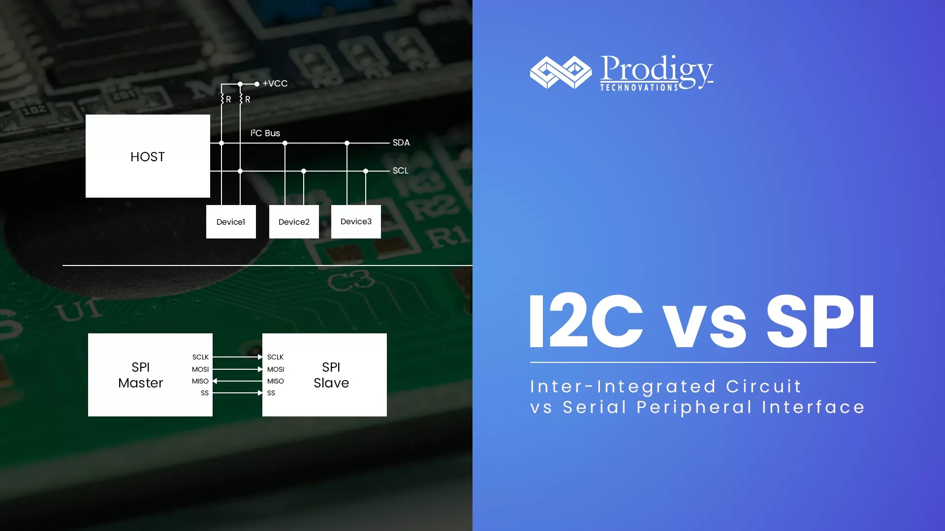
The I2C’s physical two-wire interface consists of a bi-directional serial clock (SCL) and data (SDA) lines. Each device that is connected to the bus is software-addressable by a unique address and a simple master/slave relationship with the bus exists all the time. I2C is a serial, 8-bit oriented, bi-directional data transfer that can be made at 100Kbits/s in the standard mode, up to 400Kbits/s in the Fast mode, up to 1Mbits/s in fast Mode plus, or up to 3.4Mbits/s in the high-speed mode. On-chip filtering rejects spikes on the bus data line to preserve data integrity.

Phillips Semiconductor (now NXP Semiconductors) has published I2c electrical specifications and I2c protocol specifications since 1982. The recent I2C bus specification and user manual were published in the year 2007. By following the electrical and protocol specification in the I2C document, semiconductor design, and manufacturing companies can ensure the interoperability of ICs using the I2C Bus.

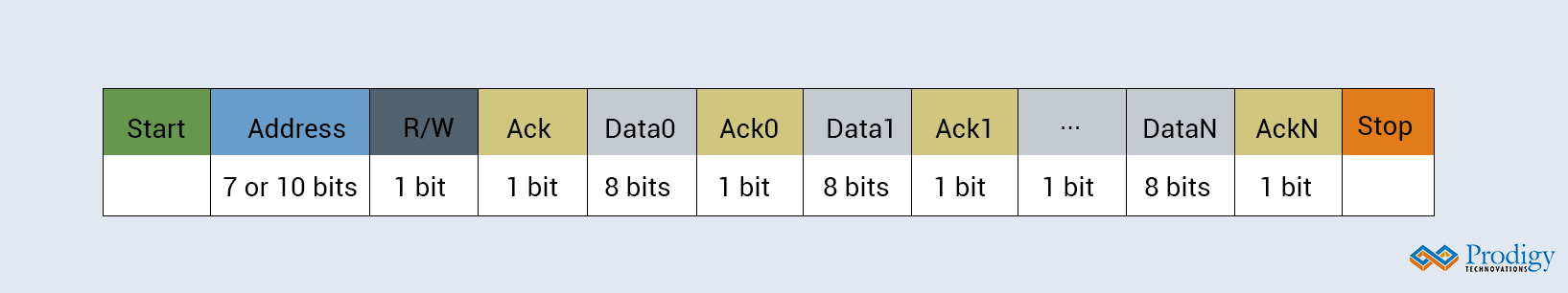
I2C protocol overview:

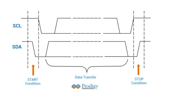
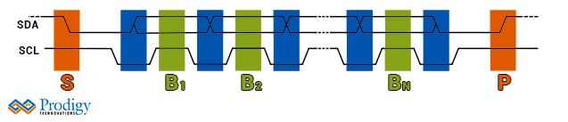
Typical data transfer between two ICs using the I2C interface is as shown:

i2c rise time, i2c setup and hold time, i2c signal integrity

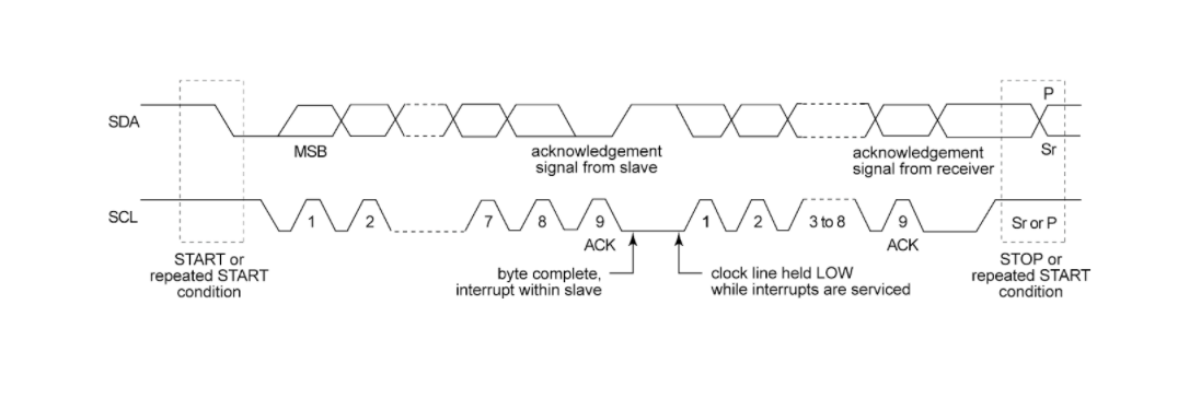
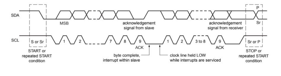
All transactions start with START Condition and stop with STOP condition In I2C Bus. These two conditions are controlled by the master IC. The typical I2C frame format has the following contents: START, address, read/write, data followed by ACK/NACK, and STOP condition at the end of the operation.

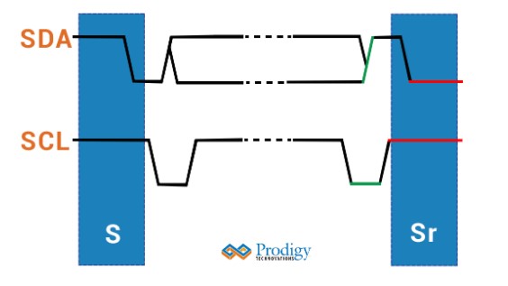
START: A condition where high to low transition of SDA line occurs when SCL is held high. The is initiated by the master IC.

Address: Master sends the slave the 7-bit or 10-bit address of the slave device

Read/write: The slave address is followed by this bit. A ZERO indicates a transmission (write), and a ‘ONE’ indicates a request for READ.

Acknowledge (ACK) and Not Acknowledge (NACK): This takes place after every byte. During this condition, the transmitter releases the SDA line during the acknowledged clock pulse so that the receiver can pull the SDA line LOW, and the SDA line remains stable LOW during the HIGH period of this clock pulse.

When SDA remains HIGH during this 9th clock pulse, this is defined as the Not Acknowledgement signal. The master can then regenerate either a STOP condition to abort the transfer or a repeated START condition to start a new transfer.

Data is an integer number of bytes read or written into a device.

STOP: A condition during SDA transitions from LOW to HIGH when SCL is held high indicating the end of a transfer of data.

I2C Bus Electrical Measurements:

For successful interoperation of IC using an I2C bus, the electrical characteristics of physical layer signals of I2C SCL and SDA signals should be compatible. The timing between the master and slave devices should be within the electrical specifications defined in the I2C Specification by NXP Semiconductor. The electrical measurement list is as follows:

Symbol Parameter Symbol Paramater
fSCL SCL Clock Frequency tr rise time of both SDA and SCL Signals
tHD;STA hold time (repeated) START condition tf fall time of both SDA and SCL signals
tLOW Low Period of the SCL clock tSU; STO set-up time for STOP condition
tHIGH High Period of the SCL clock tBUF bus free time between a STOP and START

condition

tSU;STA set-up time for a repeated START

condition

tVD; DAT data valid time
tHD;DAT Data hold time tVD; ACK data valid acknowledge time
tSU;DAT Data setup time

The detailed definitions of each of these measurements are as below:

i2c rise time, i2c setup and hold time, i2c signal integrity

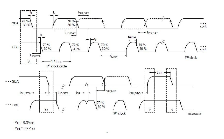
fSCL SCL Clock frequency: Inverse of one cycle period measured at 30% of the amplitude of SCL signal. It should be measured at the first cycle after the START condition.

tr, rise time of the SCL and SDA signals: time is taken by the rising edge to reach 70% of the amplitude from 30% of the amplitude of SCL and SDA signals.

tf fall time of the SCL and SDA signals: time is taken by the falling edge of the signals to reach 30% of the amplitude  from 70% of the amplitude of SCL and SDA signals

tHD;STA hold time (repeated) START condition: Minimum time the data should be low before SCL is in a low state at (repeated) START condition. It is measured as the time taken from 30% of the amplitude of SDA at high to low transition to 70% of the amplitude at high to low transition of SCL Signal.

tLOW Low period of the SCL signal: It is the minimum low time that should be maintained by the SCL signal. It is measured as half period measured at 30% of the amplitude of the SCL signal.

tHIGH High period of the SCL Signal: It is the minimum high time that should be maintained by the SCL signal. It is measured as a half period measured at 70% of the amplitude of the SCL signal.

tSU; STO Setup time at STOP condition: It is measured at STOP condition of the I2C frame. It is measured as the time between 70% of the amplitude at the rising edge of the SCL signal to 30% of the amplitude of the SDA signal at the STOP condition.

tSU;STA Setup time for repeated START condition: This measurement is carried out at repeated START conditions only. It is time measured between SCL and SDA signals at 70% amplitude of the signals.

tVD; DAT Data Valid time: Measured at every data and clock transition. This is measured concerning the 30% amplitude falling edge of SCL to 70% of the rising edge or 30% of the falling edge of the SDA signal. The I2C specification maximum allowed data valid time at different I2C speeds.

tVD; ACK data valid acknowledge time: Measured at acknowledgment bit. It is the time from 30% of the falling edge of the eighth clock from the start of data to 70% of the ack bit or 30% of the ack bit.

I2C Protocol Electrical Measurement Challenges:

During the electrical validation of the I2C bus, test engineers need to ensure the I2C bus should comply with the electrical parameters of the I2C Bus. The challenges faced while the electrical validation of the I2C bus is as follows:

  • Test/Design Engineer must know I2C Protocol behavior at the physical layer of I2C Bus
  • Electrical parameter measurements must be carried out at different protocol states (for example; stop bit, ack bit, and so forth)
  • Reference level for each of the measurement changes based on the rising or falling edge of the I2C signal transition
  • The reference level is either 30% or 70% as against the normally used reference level of 10% to 90% or 20% to 80%
  • Validation is time-consuming

Overall, measuring I2C electrical measurements demands a very high level of expertise in I2C physical layer behavior, protocol layer, signal acquisition in an oscilloscope, and I2C Electrical measurement procedures. Due to the complexity of I2C Electrical measurements, the results can be prone to errors.

The Solution to I2C Bus Electrical Measurements

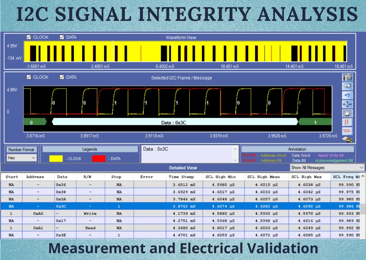
Prodigy offers I2C Electrical Validation and Protocol Decode Software to measure I2C setup and hold time, and I2C rise time. PGY-I2C Electrical Validation and Protocol Decode software offers PHY layer measurements for checking the I2C signal integrity issues.

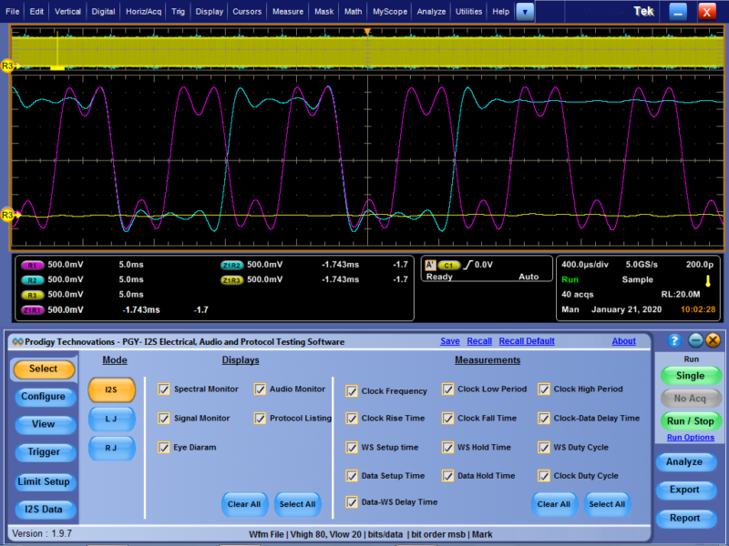
The PGY-I2C Electrical Validation and Protocol Decode Software offer electrical measurements and protocol decoding as specified in Rev 03, June 2007 I2C Bus specification. Now design and test engineers can automatically make accurate and reliable electrical measurements and decode protocols in PGY-I2C software using data acquired by Tektronix DPO5000, DPO7000, DPO/DSA/MSO70000 Series oscilloscope to reduce the development and test cycle.

PGY-I2C Software runs inside Tektronix oscilloscopes. During the run operation of the application, PGY-I2C sends commands to acquire SCL and SDA signals of the I2C bus. For accurate measurements, the recommended oscilloscope setup is:

  • The signal is at least 5 to 6 six main vertical divisions in the oscilloscope display with the appropriate volts per division.
  • Select the appropriate volts per division to display the signal with at least 5 or 6 main vertical divisions.
  • Select a sample rate such that at least 8 to 10 samples are present in the rising or falling edge of SCL and SDA signals.
  • Set record length such that at least two I2C frames are captured to make the most of I2C signals.

The PGY-I2C software analyzes the acquired data for the I2C protocol. The selected measurements are displayed as follows:

i2c rise time, i2c setup and hold time, i2c signal integrity

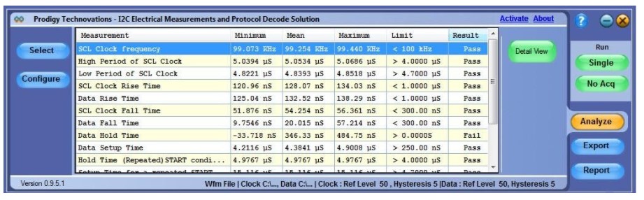
Electrical Measurement results with limits as specified in I2C standard document

The application makes each of the I2C electrical measurements in every possible I2C protocol state and displays the min, max, and mean values. If the mean value is within the limit specified, the application shows ‘Pass’. But in case, if the mean value is a pass but either the min or max values exceed the limits, applications show‘ pass*’ with an asterisk.

PGY-I2C makes all these measurements in an instant of time addressing all the challenges of I2C electrical measurements, giving accurate and reliable measurements.

Summary:

PGY-I2C Electrical Validation and Protocol Decode software offer the industry’s best I2C Electrical Validation and protocol decode software. This software allows design and test engineers to characterize the I2C bus for compliance with I2C bus standard specifications.

PGY-I2C software has the leading feature ‘Detail View’ to debug the I2C bus at the physical layer and at the protocol layer for electronic system-level development.

PGY-I2C software runs inside industry-leading Tektronix oscilloscopes such as DPO5000, DPO7000, and DPO/MSO/DSA70000 to offer the most accurate and reliable solution.

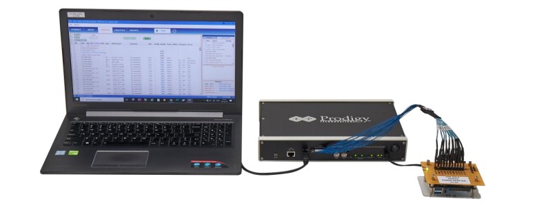
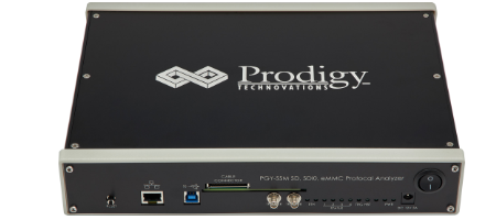
Prodigy also provides I2C Protocol Analyzer and Exerciser with multiple features to capture and debug communication between host and design under test. Prodigy’s I2C/SPI Protocol Analyzer and Exerciser is the leading instrument that enables the design and test engineers to test the respective I2C or SPI designs for their specifications by configuring the PGY-I2C/SPI-EX-PD as Master/Slave, generating I2C/SPI traffic and decoding the I2C/SPI protocol decode packets.

Have an I2c-related query?  Post here – Prodigy Forum

Introduction to I2C Bus:

I2C stands for Inter-Integrated Circuit. Philips Semiconductors developed I2C in the early 1980s as a low-cost solution for connecting lower-speed peripheral ICs to processors and microcontrollers over short distances. Since then, I2C has evolved into a worldwide standard for communication between devices in embedded systems. The simple two-wire design can be used in applications like I/O, A/Ds, D/As, temperature sensors, microcontrollers, microprocessors, etc.

I2C is a half-duplex serial communication protocol and data is transferred bit by bit along a single wire. I2C supports multiple masters and slaves on the bus, but only one master may be active at a time. Any I2C device can be attached to the bus allowing any master device to exchange information with a slave device. A device can operate either as a transmitter or a receiver depending on its function. Initially, I2C only used 7-bit addressing but evolved to allow 10-bit addressing as well. Three bitrates are supported: 100 kb/s (standard mode), 400 kb/s (fast mode), and 3.4 Mb/s (high-speed mode).

The I2C standard specifies the following format as shown below:

I2C Bus

Figure 1. I2C Frame Format

  • Start – indicates that a device is taking control of the bus and that a message will follow. 
  • Address – a 7 or 10-bit number representing the address of the device that will either be read from or written to. 
  • R/W Bit – one bit indicating if the data will be read from or written to the device. 
  • Ack – one bit from the slave device acknowledging the master’s actions.
  • Data – an integer number of bytes read from or written to the device. 
  • Stop – indicates the message is complete and the master has released the bus.

I2C THEORY OF OPERATION

I2C uses a controller known as the master to communicate with slave devices. A slave may not transmit data unless it has been addressed by the master. Each device is recognized by a unique address to differentiate between other devices that are on the same I2C bus. I2C’s physical two-wire interface consists of the bi-directional serial clock (SCL) and data (SDA) lines. Both SCL and SDA lines must be connected to Vcc through a pullup resistor. Data transfer is initiated only when the bus is idle. A bus is considered idle if both SDA and SCL lines are high after a stop condition.

I2C START AND STOP CONDITIONS

I2C communication on the bus is initiated by the master sending a START condition and terminated by the master sending a STOP condition. A high-to-low transition on the SDA line while the SCL is high defines a START condition. A low-to-high transition on the SDA line while the SCL is high defines a STOP condition.

I2C Bus

Figure 2. I2C Start and Stop Conditions

I2C REPEATED START

A repeated START condition is useful when the master wishes to start a new communication but does not wish to let the bus go idle with a STOP condition. Sending a stop condition can cause the master to lose control of the bus to another master (in multi-master environments). Hence, a repeated start condition is used. Here, instead of sending the STOP condition, the master sends another START condition followed by the address, read/write bit, and data. For generating a repeated START, the master changes the SDA line from high to low while the SCL line is high. In case the I2C bus remains busy, the master sets the SDA line to high during the low phase of the SCL to prepare for the repeated START condition.

I2C Bus

Figure 3. Repeated START Condition

I2C DATA FORMAT

One data bit is transferred during each clock pulse of the SCL. One byte consists of eight bits on the SDA line. A byte may either be a device address, register address, or data written to or read from a slave. Data is transferred to the most significant bit (MSB) first. Any number of data bytes can be transferred from the master to the slave between the START and STOP conditions. Data on the SDA line must remain stable during the high phase of the clock period, as changes in the data line when the SCL is high are interpreted as control commands (START or STOP).

I2C ACK BIT :

Each byte of data including the address byte is followed by one ACK bit from the receiver. The ACK bit allows the receiver to communicate with the transmitter that the byte was successfully received, and another byte may be sent. Before the receiver can send an ACK, the transmitter must release the SDA line. For all data bits, including the acknowledge bit, the master must generate clock pulses. If the slave device does not acknowledge the transfer, this means that there is no more data, or the device is not ready for the assignment yet. 

The 9th clock cycle of SCL is for the ACK and NACK. The acknowledge signal is valid when the transmitter releases the SDA line during the acknowledge clock pulse. If the receiver pulls the SDA line low, and it remains at a stable low during the high period of the clock pulse, it indicates ACK. If the SDA line is drawn too high, then that signifies NACK.

Several conditions lead to the generation of a NACK:

  • The receiver is unable to receive or transmit because it is performing some real-time function and is not ready to start communication with the master.
  • During the transfer, the receiver gets data or commands that it does not understand.
  • During the transfer, the receiver cannot receive any more data bytes.
  • A master receiver is done reading data and indicates this to the slave through a NACK.

I2C DATA:

Data must be sent and received to or from the slave devices, but how it is accomplished is by reading or writing to or from registers in the slave device.

Registers are locations in the slave’s memory that contain information. Information can be in the form of configuration or some data that is to be sent back to the master. The master must write information into these registers to instruct the slave devices to perform a task.

Figure 4. Data Transfer using the I2C Interface

DEBUG TOOLS FOR I2C Bus: HOW TO DEBUG I2C Bus:

Prodigy also offers an I2C Protocol analyzer to capture and decode the I2C packets. The I2C protocol analyzer has the advanced capability not only to trigger but long allow very long captures which is very useful for the embedded design engineer during the debugging.

I2C Protocol Analyzer

Prodigy I2C Protocol Analyzer

Have an I2c-related query?  Post here – Prodigy Forum

About the Author

Raghavendra Bhat is an Application Engineer at Prodigy Technovations. He graduated from NMAM Institute of Technology in 2020 with a bachelor’s degree in Electronics & Communication Engineering. His area of interest includes Embedded systems, Digital System Design, and Automotive Electronics.

For more information reach out to us at (contact@prodigytechno.com)

I2S Protocol Introduction

Today’s digital systems – from the Digital TV in the living room, Alexa, and google home for playing music and switching from text-based search to voice-based search– are driving convergence on many fronts. Quality of Experience is taking center stage. Audio requirements in Computers, Mobile Handsets, and Home Automation products have changed dramatically. Audio content to and from the processors is increasingly becoming digital data.

I2S Standard: Theory of Operations

The digital audio signals in most systems are being processed by several devices, such as ADCs, DACs, DSPs, Digital I/O interfaces, and many more. To enhance flexibility and interoperability, it is critical to have standardized communication structures, for both the equipment and the silicon developers.

Inter-IC Sound (I2S) bus – a serial link, is developed especially for digital audio. The bus handles only audio data through a simple, 3-line serial bus consisting of:

•  Continuous Serial Clock (SCK);
•  Word Select (WS); and
•  Serial Data (SD)

The Clock

The transmitter and receiver have the same clock signal for data transmission. Typically, the transmitter acts as the master and generates the bit clock, word-select signal, and data. The slave derives its internal clock signal from an external clock input. In complex systems having several transmitters and receivers, a system master controls digital audio data flow between various ICs.

For data and word-select inputs, the external to internal clock delay is of no consequence because it only lengthens the effective set-up time. The major part of the time margin is to accommodate the difference between the propagation delay of the transmitter, and the time required to set up the receiver.

All timing requirements are specified relative to the clock period or the minimum allowed clock period of a device. Thus, higher data rates can be used in the future.

Word Select

The word select line indicates the channel being transmitted:

•  WS = 0; channel 1 (left);
•  WS = 1; channel 2 (right).

In the slave, this signal is latched on the leading edge of the clock signal. The WS line changes one clock period before the MSB is transmitted. This allows the slave transmitter to derive synchronous timing of the serial data that will be set up for transmission. Moreover, it enables the receiver to store the previous word and clear the input for the next word.

Serial Data

I2S Protocol offers a very high degree of flexibility. The transmitter and receiver may have different word lengths. Also, the transmitter doesn’t need to know how many bits the receiver can handle, nor does the receiver need to know how many bits are being transmitted.

To enable this, the Serial Data is transmitted in two’s complements with the MSB first. The MSB has a fixed position, whereas the position of the LSB depends on the word length. When the system word length is greater than the transmitter word length, the word is truncated (LSB set to ‘0’) for data transmission. If the receiver gets more bits than its word length, the bits after the LSB are ignored. In case the receiver is sent fewer bits than its word length, the missing bits are set to zero internally.

Challenges in Debug I2S Protocol:

The key performance of current-generation digital Audio is measured based on the quality of output audio, battery life, and portability. To achieve these performance factors, the industry converts the analog audio signal into digital to reduce the effect of SNR and also employs multiple digital signal processing algorithms to create a compelling audio experience. To enhance the battery life, the designer pursued chips designed based on power-aware technology. This technology turns on and off the different blocks within an IC.

These design practices throw up the following challenges to designers.

•  Debugging the content of the Audio Serial buses
•  Ensuring physical layer timing and compliance with standard
•  Ensure very high-level signal fidelity during the signal transformation from Analog to Digital and vice versa.
•  Reducing the noise components generated due to mixed-signal design and new generation power-aware ICs.
•  Interoperability of different vendors Audio subsystems
•  Maximize the design margins with low power and voltage

Traditionally often, engineers use multiple instruments such as an Audio analyzer for dealing with audio domain-related challenges, a logic analyzer for dealing with link-layer challenges, and Oscilloscopes for dealing with signal integrity and timing challenges. Involving multiple instruments adds additional complexity to the test setup.

Now a single tool arrives to address all of the above challenges in the I2S protocol design. PGY-DAA I2S Digital Audio Analysis software along with the Tektronix Oscilloscope is a single tool to cross-examine the protocol layer and the PHY layer while verifying the audio performance and helps to address all the challenges listed above.

I2S Protocol

Summary

PGY-I2S I2S Audio / Protocol Decode / Electrical Test Software along with the Tektronix DPO7000, DPO/MSO70000/B series oscilloscope offers a comprehensive set of tools that enables design and validation engineers to efficiently, and effectively, debug the toughest I 2 S challenges.

Difference between I2C vs I2S

What is I2C Protocol?

I2C stands for Inter IC communication. I2C is a simple two-wire protocol used to comminute between two devices or chips in an embedded system. I2C has two lines SCL and SDA, SCL is used for the clock, and SDA is used for data.

i2c vs i2s

I2C Timing Diagram

What is I2S Protocol?

Inter-IC Sound (I 2 S) bus – a serial link, is developed especially for digital audio. The bus handles only audio data through a simple, 3-line serial bus consisting of:

  • Continuous Serial Clock (SCK);
  •  Word Select (WS); and
  •  Serial Data (SD)

i2s

The timing diagram for I2S

What is the difference between I2S and I2C (I2C vs I2S)?

● I2C is used to connect to general inter-IC communication ie EEPROM or sensors and I2S is used only for audio devices

● I2C supports multi-master and multi slave and I2S supports single master

● I2C is 2 wire protocol and I2S is 3 wire protocol.

● I2C supports clock stretching and I2S does not have clock stretching.

● I2C has an extra overhead start and stop bits and I2S does not have any start and stop bits.

● I2C has acknowledgment communication after every byte of the transfer

● I2C has a pullup resistor requirement.

Advantage I2C:

● Easy device add-on: It’s easy to add a new slave device to the bus. Just add the new device without adding a new select like, unlike SPI.

Advantage I2S :

● Audio: It delivers a full audio chain and eliminates the need for any preamplifier and DAC and ADC

What is the Protocol Analyzers to Debug I2C Protocol?

Prodigy offers a protocol analyzer to capture and monitor I2C Bus. I2C protocol analyzer, has advanced capability not only to trigger but long allow very long captures which is very useful for the embedded design engineer during the debug.

I2C/SPI Exerciser and Protocol Analyzer

Have an I2c-related query?  Post here – Prodigy Forum

The Differences between eMMC and UFS are:

What is eMMC Protocol?

Embedded multimedia card or eMMC, is a NAND flash memory for mobile applications and a memory solution for consumer electronics such as tablets, smartphones, GPS systems, eReaders, and other mobile computing devices.

What is UFS Protocol?

Universal Flash memory or UFS is the next generation of Flash memory. UFS is providing flash memory with high data transfer speed, high reliability, and low power consumption. The UFS standard is managed and developed by the JEDEC. UFS 4.0, the most advanced JEDEC standard, offers sequential read-write speeds to support live streaming and augmented reality applications in mobile devices. UFS will be the next-generation flash memory standard for automotive applications as well.

What is the difference between eMMC and UFS ( eMMC vs UFS )?

  • UFS has Low voltage differential Signalling (LVDS) signaling interface.
  • UFS has a command Queue (CQ) to sort out commands to be carried out and allow multiple commands to be carried out.
  • eMMC is half-duplex hence either read or write into the memory is possible.
  • UFS is a full-duplex interface and allows simultaneous read and write.
  • eMMC is slower than UFS.
  • UFS supports advanced features like Deep Sleep, write booster, and throttling notifications to the host.

Advantage eMMC

  •  Cost: eMMC continues to be cheaper and most widely used in smartphones and most consumer devices as storage devices.

Advantage UFS :

  • Speed: UFS 4.0 can support bandwidth up to 4800 MB/s

What is the Protocol Analyzers to Debug eMMC Protocol and UFS Protocol?

Prodigy offers a protocol analyzer to capture and monitor eMMC and UFS packets. Prodigy’s eMMC protocol analyzer and UFS 4.0 protocol analyzer has the advanced capability not only to trigger but long allow very long captures which is very useful for the embedded design engineer during the debug. UFS4.0 protocol analyzer comes with advanced series of probes to capture high-speed signals.

UFS 4.0 Protocol Analyzer

UFS4.0 protocol analyzer

INTRODUCTION

A startup was working on AI Edge-based voice processor chip. The voice-based AI chip is designed to consume the lowest power as it’s used in consumer headphones or earbuds. The startup was about to tape out the chip and was preparing for a post-silicon bring-up. It faced very significant barriers in the development phase with I/O peripherals like I2C and SPI and using Prodigy protocol analyzer and exerciser it was able to quickly solve some challenges and get ready for the post-silicon validation. The older generation chip was done in 40nm and the latest migration after testing and getting the confidence was to migrate to a 7nm process node.

THE AI PROCESSOR

The AI processor is one of the first-generation chips that enables complete voice control for consumer products. The consumer devices can be smart speakers, remotes, earbuds, and automotive solutions. The AI processer does the inference and training to enable autonomous speech recognition without sending audio to the cloud for further processing.

 The AI Processor details are as follows:  

Key Features:

  • 5 AI cores provide 1028 MAC operations per clock cycle
  • 60 uW active power consumption in inference tasks
  • Sensor fusion with 8 I/Os
  • Years of operations on a coin cell battery
  • Ultra-low-power ADCs
  • 5nm process node

Architecture Diagram :

Architecture Diagram

Development Challenge

The startup was in the tape-out phase of its design when it approached Prodigy Technovations for solutions to help them verify the feasibility of its design. One of the major requirements was to help in testing their standard peripherals which would be used in conjunction with the AI processor using serial communication protocols like I2C, SPI, QSPI, and I2S. The peripherals in the picture were EEPROMs, SDIO’s, and FLASH memory which were being used in applications involving video processing and sensor fusion. The AI processor was to act as the master and the consecutive peripherals as slaves. 

Hence, Prodigy’s I2C SPI Exerciser and Protocol analyzer proved to be a handy tool in debugging design issues and observing how the slaves behave under different test cases our product was capable of generating. In this case, the prodigy I2C SPI protocol analyzer would help with decoding the protocol bus and reporting and monitoring, and capturing any bus transaction-level issues.

Also, another requirement put forward was to be able to use the Prodigy I2C SPI Exerciser as a slave and their AI-based processor as a master, to observe different scenarios and do the timing control on bus signals and also improve any development issues on the peripheral during the post-silicon bring up. 

Some of the key changes for SPI and I2C Protocol were 

  1. Provision for BYTE timing delay and delay between transactions.
  2. Validation of Basic read and write test transactions and integration them via API into the development flow to automate testing

Problem Solved and Key Learnings 

The slaves used were I2C Atmel and SPI Winbond. The read and write operations were not in a proper sequence. On investigation using the protocol analyzer and exerciser, it was found that the datasheets of the corresponding slaves were not referred to by the design team. The Prodigy protocol analyzer and exerciser were not only able to debug the issue but also gave the flexibility to figure out issues in the development team. Check out our protocol analyzer and exercisers.

Where is Logic Analyzer used?

Embedded System Testing :

Embedded Systems have multiple devices and each of the devices uses the bus to communicate with the main chip or processor and other devices in the system. The Embedded system generally has SPI and I2C devices to communicate with the main processor. A logic analyzer can be very useful to debug and validate the embedded system and figure out failures of any of the devices in the embedded system.

Post-silicon validation:

During the chip development process, Once the Chips is back from the foundry all the interface of the Chip or SoC needs to be tested. Most of the SoC or chips have I2C, SPI, and UART interfaces. The logic analyzer is a very handy tool for the hardware validation engineer to debug all the various digital channels of I2C, and SPI failures.

Pre-Silicon validation:

In chip or SoC development, before the chip is taped out its engineering manager needs to get the confidence development of the chip, Emulation platforms like Zebu or Palladium are commonly used to do the hardware validation.  A logic analyzer can be a very useful assist tool for the emulation engineer to check for the sanity of the communication interface like I2C and SPI along with the emulation Platform.

What are the various Features of a Logic analyzer?

Logic Analyzer comes with the following features:

  • Channel Count: The maximum number of digital channels supported by the logic analyzer. The more the channels the more debug capability.
  • Triggering: Each of the logic analyzers and equipped with various kinds of triggers, multi-level triggers, multiple consecutive event triggers, etc.
  • Sample Rate: This is defined by the maximum frequency that can be measured by the logic analyzer.
  • Channel Bandwidth: The logic analyzer needs to have the ability to capture glitches, setup, and hold time issues in the embedded design. The lower the resolution of measurement by the logic analyzer the better the issues that can be captured in the design.

How to integrate a Logic analyzer in the Development Environment?

The Channels which are being measured need to be connected directly to logic analyzer probes. The logic analyzer also provides access to API libraries. These APIs can be integrated into the development environment and an advanced level of validation and testing can be achieved.

What is Prodigy doing to advance in the logic analyzer Market?

Prodigy Technovations regularly looks at the new trends in the market and comes up with a new set of products for the logic analyzer market. Prodigy Technovations has an expert team working on the latest cutting-edge technologies and Prodigy Technovations is going to lead the market in the pc based logic analyzer market in the coming years.

<HOME

Request For Quote

Share your requirement and our team will provide a tailored quote based on your validation needs.

"*" indicates required fields

This field is for validation purposes and should be left unchanged.
Address*

Request For Demo

Tell us your use case and our team will schedule a product demo aligned to your validation workflow.

"*" indicates required fields

This field is for validation purposes and should be left unchanged.
Address*

Request A Demo

Tell us your use case and our team will schedule a product demo aligned to your validation workflow.

"*" indicates required fields

This field is for validation purposes and should be left unchanged.
This field is hidden when viewing the form
Address*

Request Quote

Share your requirement and our team will provide a tailored quote based on your validation needs.

"*" indicates required fields

This field is for validation purposes and should be left unchanged.
Address*