What is I2C Protocol?

I2C stands for Inter IC communication. I2C Protocol is a simple two-wire protocol used to communicate between two devices or chips in an embedded system.

What is I3C Protocol?

I3C has got the extra I over the standard I2C. Improved Inter IC communication protocol. I3C Protocol has improved over I2C Protocol in many ways. I3C Protocol maintains the backward comparability with I2C Protocol. However, it provides advanced features required for modern communication w.r.t to speed and interrupts handling, etc.

What is the difference between I3C vs I2C Protocol?

The difference between I3C vs I2C can be understood by knowing the details of the protocol. While some differences are very obvious like improved speed and backward compatibility there are very interesting features worth understanding. The differences are:

  • I3C is power efficient and high speed compared to I2C.
  • I3C supports single data rate (SDR), High Data rate (HDR) modes, through which it can support up to 33Mbps data rate whereas typical I2C network support up to 1Mbps.
  • In I2C, all the operations will happen with static address whereas in I3C, I3C master will assign dynamic address to all the slaves present on the bus.
  • Dynamic address assignment for I3C slaves but still supports static address for I2C slaves.
  • I3C has a standardized set of common command codes (CCC). There are three types of common command codes: Broadcast commands, Directed commands, and private.
  • Broadcast commands are like a master, which will send CCC to all the slaves to set the same register value for all slaves present on the I3C bus.
  • Directed commands are like a master, which will send CCC to the specific slave to read/write register from the slave.
  • I3C supports In-band interrupt (IBI) on the I3C bus. So separate pins are not required.
  • I3C master will assign a dynamic address to the slave as per the priority of the slave. In such cases, the master depends on reading PID, BCR, and DCR registers from the slave and it will assign a dynamic address to the slave ever slave has the lowest dynamic address has the highest priority on the bus. Because any transaction start initially it will be in open drain mode so in that phase any slave or secondary master can give the IBI or secondary master request whoever wins the arbitration will complete the transaction on the I3C bus.
  • I3C supports a hot join operation in which the slave will send a hot join request to the master and the master will assign a dynamic address to the slave.
  • I3C has error detection and recovery (parity check in SDR, parity, and 5bit CRC for HDR modes).
  • Multi-master operation with well-defined ownership transfer from one master to another master.

What is the Protocol Analyzers to Debug I3C vs I2C Protocol?

Prodigy offers I3C Protocol Analyzer with advanced capability to trigger and capture the I3C protocol based on I3C Protocol specification.

Prodigy I3C Protocol Analyzer 


I3C vs I2C Protocol Analyzer

Prodigy also offers an I2C Protocol analyzer to capture and decode the I2C packets. The I2C protocol analyzer has the advanced capability not only to trigger but long allow very long captures which is very useful for the embedded design engineer during the debug.

Prodigy I2C Protocol Analyzer


I3C vs I2C Protocol Analyzer


Conclusion

In conclusion, I3C vs I2C protocol analyzer choice depends on factors like cost and current design. However, the I3C protocol is gaining traction and will be the de facto interface for most of the chipsets developed in the future. To Read more Blogs on Protocol Analyzer, Click Below.

Have an I2c-related query?  Post here – Prodigy Forum

<PROTOCOL ANALYZERS

How to Choose a Logic Analyzer?

If you are in the market for buying or choosing a Logic Analyzer, how do you know which one is right for you? There are several options to select from and looking at the various technical specifications can be a daunting task. This article gives you some factors to consider when considering your purchase.

  • Channel Count: The maximum number of digital channels supported by the logic analyzer. The more the channels the more debug capability. Typically a logic analyzer has around 8 Channels. It’s always good for logic analyzers to have more channels based on the complexity of the embedded design.
  • Channel Bandwidth: This can be defined by the maximum frequency that can be measured by the logic analyzer.
  • Sample rate: The Logic Analyzer needs to have the ability to capture glitches, setup, and hold time issues in the embedded design. Lowering the resolution of measurement by the logic analyzer, better the issues that can be captured in the design.
  • Voltage Levels: The digital design comes with various logic levels. The Logic Analyzer needs to support logic families to debug the embedded system design. It’s always good to understand the voltage levels of the design and logic analyzer.
  • Trigger Capability: A good Logic Analyzer can set complex and nested triggers. Understanding the trigger level and capability will help you select the right logic analyzer for you.
  • Probe Type: The Logic Analyzer probes need to be easily connected to the design under test without creating any signal integrity issues.
  • Capture duration: During complex engineering debugging a very long capture sequence is required to do the analysis. Hence having a very large capture can be an added
  • Host Interface: USB 2.0 is the most commonly used interface for the logic analyzer some of them also have interfaces to the network using gigabit Ethernet.

Other Features to Consider:

  • Support: Once you have the Logic Analyzer in your hand and run into issues during debug you will need a good team to support the debug issues in hand. Every company offers various levels of support.
  • Shipping Lead Time: Once the logic analyzer is ordered the product needs to be shipped to the development location. Please check the lead times well in advance before ordering.
  • Year of development: It’s always good to pick up a product that is stable in the market and used by many customers already.
  • Ease of Use: Most of the Logic Analyzers are used to debug hard engineering problems and ease of use and integration into the development environment are very important features for the product.

Conclusion:

Shopping or choosing of Logic Analyzer can be a daunting task, and this guide will help you easily navigate the process of selecting the logic analyzer. As the number of channels to debug increases so does the cost of the product.

Prodigy offers Logic Analyzer which supports Real-time I3C Trigger & Protocol Analysis which enables engineers to debug timing, circuit-level, and system-level problems quickly. Advanced trigger, streaming, and unlimited data capture capabilities make it a must-have tool in your lab to debug I3C protocol.

Prodigy’s Logic Analyzer performs simultaneous protocol analysis of #I3C, #I2C, #SPI, #UART, #SPMI, #CAN/CAN FD, and #RFFE in embedded designs. Features such as 16 channels, 1GS/s Timing Speed, 2ns glitch Analysis & 100MHz state data capture make it an ideal must-have debug tool to address digital design problems. Designers can now easily analyze setup and hold time issues, glitches, and synchronous data activities apart from analyzing protocol issues.

A logic analyzer is an electronic instrument that captures and displays multiple signals from a digital system or a digital circuit. It is an excellent tool for verifying and debugging digital designs. A logic analyzer may convert the captured data into timing diagrams, protocol decodes, state machine traces, and assembly language. For debugging elusive, intermittent problems, some logic analyzers can detect glitches, as well as setup-and-hold time violations. During software/hardware integration, logic analyzers trace the execution of the embedded software and analyze the efficiency of the program’s execution. Some logic analyzers correlate the source code with specific hardware activities in your design.

Prodigy’s Logic Analyzer supports Realtime I3C Trigger & Protocol Analysis.

Why use a logic analyzer?

Debugging microprocessor-based designs required more inputs than what conventional analog oscilloscopes could offer. A typical logic analyzer has anywhere from 8 to 136 channels and they are particularly useful for looking at time relationships or data on a bus – for example, a microprocessor address, data, or control bus. They can decode the information on microprocessor buses and display it in a meaningful form.

A logic analyzer is used when we need to:

– Debug and verify digital system operation
– Trace and correlate many digital signals simultaneously
– Detect and analyze timing violations and transients on buses
– Trace embedded software execution

Types of Logic Analyzers:

There are three types of logic analyzers: Modular logic analyzers, Portable logic analyzers, and PC-based logic analyzers.

Modular Logic Analyzers:

Modular logic analyzers are the standard form seen in labs that have a chassis and multiple modules. These are one of the more expensive and provide the highest level of functionality to the user. Modules can be added or removed depending on the user to increase the functionality. Eg: Modules can be added to increase the number of channels in the Logic Analyzer depending on the user.

Portable Logic Analyzer:

Portable logic analyzers are more portable than modular logic analyzers and provide all the functions that are integrated into a single module with a screen. There may be instances when a smaller analyzer will be required due to restricted budgets or fields of service. These test instruments incorporate all elements of the analyzer into a single unit for ease of transportation.

PC-based Logic Analyzer:

PC-based logic analyzers are compact and they directly interface to a computer via an ethernet or a USB cable. The captured information is displayed to the user via the PC’s display. PC-based logic analyzers are the least expensive but are limited in terms of power compared to modular and portable logic analyzers.

Prodigy’s Logic Analyzer supports Real-time I3C Trigger & Protocol Analysis which enables engineers to debug timing, circuit-level, and system-level problems quickly. Advanced trigger, streaming, and unlimited data capture capabilities make it a must-have tool in your lab to debug I3C protocol.

Perform simultaneous protocol analysis of #I3C, #I2C, #SPI, #UART, #SPMI, #CAN/CAN FD, and #RFFE in embedded designs. Features such as 16 channels, 1GS/s Timing Speed, 2ns glitch Analysis & 100MHz state data capture make it an ideal must-have debug tool to address digital design problems. Designers can now easily analyze setup and hold time issues, glitches, and synchronous data activities apart from analyzing protocol issues.

<PRODIGY’S LOGIC ANALYZER

Evolution of Logic Analyzers: Future of Logic Analyzers in embedded system design

Traditionally Logic Analyzers are used to monitor parallel buses in microprocessors, microcontrollers, or PATA or memory interface-based designs. Data transfer between microprocessor and peripherals ICs is using the parallel bus. Programming of microprocessors or microcontrollers used to be in assembly language. To support debug digital design Logic Analyzers provided 100s of channels, advanced parallel pattern triggers, long acquisition memory, and disassemblers for different microprocessors and microcontrollers. Disassembler is additional hardware commonly called ‘PODS’ used to capture the data in microprocessor/microcontrollers IOs. Software associated with the POD is used to disassemble the captured data and display it in assembly language. This runtime assembly language code is used to provide great details enabling designers to debug and optimize the designs.

But modern electronics designs moved away from parallel bus design for good and adapted serial bus architecture for low-speed, high, and ultra-high-speed designs. Current digital designs are based on a system on a chip that has multiple low-speed and high-speed serial bus interfaces to support different design needs.  Data transfer between ICs or peripherals takes place using protocol using the serial bus. Product differentiation is driven by software features which continuously updated to add more capabilities. This has driven demand for a different set of capabilities in Logic Analyzer. To support these design needs Logic Analyzer does not need to be a high channel count but it should be capable of capturing data from multiple serial bus designs and displaying it in a time-correlated form so that designers can visualize the system-level operation. But just viewing the digital waveforms it is extremely difficult to interpret the serial data. Hence Logic Analyzer should provide multiple serial bus decoding capabilities. This simplifies the entire debug process.

Debugging any design is a very challenging activity. Designers need to find the root cause using the symptoms such as bus failure, boot failure, etc. Designers try to narrow down by eliminating different possible causes of the symptoms by looking at specific data and analyzing them. To get to the specific cause, the Logic analyzer should have the capability to define triggers on specific events or the ability to look for multiple events and take smart actions so that the root cause of the systems can be found.

This New generation Logic Analyzer supports the following capabilities.

  • Good enough channel count (could be 10 to 32)
  • Serial bus data analysis for different Protocols
  • Simultaneously decode multiple Protocols
  • Protocol-aware trigger capabilities
  • Long acquisition support with pre and post-trigger capabilities

Prodigy Technovations offers Logic Analyzer to debug design in embedded system design. The logic analyzer is equipped to handle complex engineering problems.

Logic Analyzer for Embedded Interfaces

Logic Analyzer for Embedded Interfaces

What is UFS Protocol? What is its connection with 5G?

The arrival of 5G is changing the way the smartphone is being used and leading the way to the next generation of mobile technology. The smartphone vendors are planning to offer seamless and immersive experiences on mobile devices. 5G offers ultra-fast transfers, low latency, and low power consumption on mobile devices. These high-speed data transfers mandate the need for high-speed storage interfaces such as UFS 4.0/3.0 on mobile devices.

UFS stands for Universal Flash storage and offers more high-speed data processing than its predecessor, eMMC. This high-speed data transfer enables next-generation experiences such as 8K multimedia streaming and paves the way for augmented reality and Virtual reality experiences.

What does UFS 4.0 mean?

UFS 4.0  specification supports three new features:

  • Write Booster: This is designed to increase write speeds by using a pseudo-SLC cache. Similar technology is already present with current-generation SSDs.
  • Deep  Sleep: The new lower power state designed for the UFS devices that use the same voltage regulators for storage and other functions.
  • Performance  Throttling  Notification: This enables the UFS device to inform the host about performance throttling when overheating.

UFS 4.0 is the next-generation standard after UFS 2.0, UFS 3.1. UFS 4.0 has a very advanced capability to support 5G experiences. UFS 3.1 supports 128,256,512 GB of storage capacity. The data download capacity is up to 1200 MB offering gigabytes of sequential write speeds. UFS 3.1 also supports random read and random write of from 63000 to 68000 IOPS.

How to Debug UFS 4.0?

UFS 4.0 Protocol Analyzer

UFS 4.0 Protocol Analyzer 

UFS 4.0 debugging is a challenge as it’s very high-speed data transfer. Prodigy offers state-of-the-art debug hardware to Debug UFS protocol.

UFS 4.0 Protocol Analyzer comes with the following features:

  • Supports version MPHY 5.0, UniPro 2.0, and UFS v2.1/3.1/4.0
  • Supports PWM G1 to G7 and HS G1, 2, 3, 4, 5 Rate A and B Series
  •  Supports one/two data lanes (2 TX and 2 RX)
  • Flexibility to capture very large data using continuous streaming of Protocol data to host computer with 16GB Internal acquisition memory field upgradeable up to 64GB.
  • Hardware-based resizable circular buffer with pre/post-trigger.
  • Flexibility to decode selected data from a 16GB buffer.
  • Solder down active probe provides high signal fidelity.
  • Decoding at MPHY, UniPro, and UFS layers.
  • Trigger-based on MPHY, UniPro, and UFS layers packet content.
  • Trigger out a signal at the trigger event allows the triggering of other instruments such as an oscilloscope.
  • Interface to host system using USB 3.0.
  • Flexibility to upgrade the hardware firmware using the GbE interface provides easy field up-gradation of FPGA firmware.
  • Decoded data packets can be exported to a text file for further analysis.
  • Lightweight and can be deployed for on-site/ field tests.

SPMI Protocol Introduction

The complexity and performance requirements of mobile phones and other portable electronic devices are increasing at an exponential rate. As the demand for new high-performance, high-data-rate feature increase, system-level power management becomes critical. The use of advanced power management techniques to reduce power consumption and improve battery life is becoming more important than ever before.

To minimize the power consumption of digital processors in portable electronic devices, system, and IC designers are now using advanced power management techniques. Advanced hardware and software techniques are now being used to:

  • Accurately monitor and control processor performance level required for a given workload or application.
  • Control various supply voltages based on the performance level Rapid deployment of such advanced power management techniques requires interface standardization. This System Power Management Interface Protocol (SPMI Protocol) Specification addresses hardware interface standardization.

 What is SPMI Protocol?

The System Power Management Interface Protocol (SPMI Protocol ) is a MIPI standard interface that connects the integrated Power Controller (PC) of a System-on-Chip (SoC) processor system with one or more Power Management Integrated Circuits (PMIC) voltage regulation systems. SPMI Protocol enables systems to dynamically adjust the supply and substrate bias voltages of the voltage domains inside the SoC using a single SPMI Protocol bus. 

Within the PC of SoC, the SPMI Protocol-related functions are referred to as “Master”. Within PMIC, the SPMI Protocol related functions are referred to as “Slave”. There can be up to 4 Masters and up to 16 Slaves. Multiple Masters and Slaves can reside on a single IC, on several ICs, or on any combination of the two.

SPMI Protocol

(fig:1)

SPMI Protocol has a wide range of applications that are spread across industries that needs better Power Management. SPMI Protocol is used in Smartphones, Wearables, and other portable electronic devices. Smartphones & Wearables use SPMI Protocol for controlling the power of sensors. High-end smartphones already have multiple devices in the designs & can require up to 20 signal lines. Each of these having independent power pins can cause issues. Similarly, most portable electronic devices would need a power management interface to optimize energy consumption and reduce pin count. This requires a standardized advanced power management interface.

SPMI Protocol: Theory of operation

SPMI Protocol is a two-wire serial interface for advanced power management that connects the integrated Power Controller of an SoC processor system with one or more Power Management Integrated circuits (PMIC) voltage regulation systems. The bi-directional two lines represent the SDATA & SCLK. SDATA is a bi-directional data line and the SCLK is controlled by the master.

The SPMI protocol has the following features 

  • Bus Arbitration is the process where the bus shall be allocated to one Master or Request capable Slave among the devices that may simultaneously request to send a command sequence on the bus.
  • Master connection and disconnection – A process for a Master to connect to, & disconnect from, an initialized or uninitialized SPMI Protocol bus
  • Slave-initiated communication – A process for a Request Capable Slave (RCS) to initiate communication with a Master or other Slaves.
  • There are two defined SPMI Protocol device classes:
  • High-speed (HS): 32 KHz to 26MHz, with load up to 50 pF
  • Low speed (LS): 32KHz to 15MHz, with load up to 50 pF
  • ACK/NACK for robust communication.

The sequences shall be comprised of the following five events that occur in order:

  1. Bus Arbitration
  2. Transmission of the Sequence Start Condition (SSC)
  3. Transmission of Frames (Command Frame and one or more Data frames)
  4. Transmission of ACK/NACK for command sequences.
  5. Transmission of a Bus Park Cycle

The last four events SSC, Command/Data Frames, ACK/NACK & Bus Park Cycle together form the command sequence. The SPMI Protocol specification constructs all command sequences on the interface using individual bits.

The Sequence Start condition shall be a unique condition on the bus identified by a rising edge followed by a falling edge on SDATA while SCLK remains at a logic low level. The SSC is used by a Slave or master to identify the start of a command sequence. SDATA is driven by the Bus Owner Master to a logic level one for one SCLKint period, then to logic 0 levels for one SCLKint period while holding the SCLK at logic zero.

There are three basic types of frames: 

  • Command Frame shall consist of 13 bits with a 4-bit address field, an 8-bit command field, and a single parity bit.

SPMI Protocol

(fig:2)

OR

SPMI Protocol

(fig:3)

  • Data and Address frames consist of 9 bits with 8 bits of data or address and a single parity bit.

SPMI Protocol

(fig:4)

  • No Response Frame of 9-bits long if it is a Data Frame or 13-bits if it is a command frame.

SPMI Protocol

(fig:5)

Bus Arbitration is used to determine access to a bus for Master/s or Slave/s. Bus Owner Master monitors the arbitration and determines who gets access to the Bus. The different Bus arbitration levels are exposed after arbitration request in order as shown in the image below.

SPMI Protocol

(fig:6)

Debugging SPMI Protocol :

Prodigy’s SPMI Exerciser and Protocol Analyzer play an important role in helping the design/ test engineers test their SPMI Protocol designs based on the SPMI specification. The typical test setup for testing Master or Slave is as below.

SPMI Protocol

(fig:7)

SPMI Protocol DUT can be an SPMI Protocol Primary Master, Secondary Master, Request Capable Slave, or Non-Request Capable Slave. The software that runs in the host computer enables the user to configure the device as either a master or slave based on the requirement in DUT by selecting the appropriate selection.

SPMI Protocol

SPMI Exerciser and Protocol Analyzer

SPMI Software

SPMI Electrical Validation and Protocol Decode Software 

SPMI Protocol Signals can be initiated by using the GUI or custom SPMI Protocol packets can be initiated by writing or using existing scripts from the exerciser panel. On generating the SPMI Protocol signals, the protocol analyzer captures the exchange of SPMI Protocol packets between master and slave. The captured information is decoded and listed in the decoded result view panel and the plot is made in the timing diagram window.  

Conclusion

Prodigy offers an SPMI Protocol analyzer to help debug designs with the SPMI Protocol interface. Prodigy has a team of experienced engineers working on advanced debug interfaces and protocols to help design engineers. 

<SPMI PROTOCOL ANALYZER

A logic analyzer is an electronic instrument that captures and displays multiple signals from a digital system or a digital circuit. It is an excellent tool for verifying and debugging digital designs. A logic analyzer may convert the captured data into timing diagrams, protocol decodes, state machine traces, and assembly language. For debugging elusive, intermittent problems, some logic analyzers can detect glitches, as well as setup-and-hold time violations. During software/hardware integration, logic analyzers trace the execution of the embedded software and analyze the efficiency of the program’s execution. Some logic analyzers correlate the source code with specific hardware activities in your design.

A logic analyzer is used when we need to

  • Debug and verify digital system operation.
  • Trace and correlate many digital signals simultaneously.
  • Detect and analyze timing violations and transients on buses.
  • Trace embedded software execution.

THE LOGIC ANALYZER

Debugging microprocessor-based designs required more inputs than what conventional analog oscilloscopes could offer. A typical logic analyzer has anywhere from 8 to 136 channels, and they are particularly useful for looking at time relationships or data on a bus. For example, a microprocessor address, data, or control bus. They can decode the information on microprocessor buses and display it in a meaningful form.

LOGIC ANALYZER

A logic analyzer measures and analyzes signals differently than an oscilloscope. The logic analyzer does not measure analog details. Instead, it detects logic threshold levels. When we connect a logic analyzer to a digital circuit, we are only concerned with the logic states of the signal, i.e., a logic analyzer looks for just two logic levels. When the input is above the threshold voltage (V) the level is said to be a “high” or “1”; conversely, the level below Vth is a “low” or “0”. When a  logic analyzer samples input it stores a “1” or a “0” depending on the level of the signal relative to the voltage threshold.

HISTORY OF LOGIC ANALYZER

Circuits started becoming smaller after the invention of the Integrated circuit (IC) in the early 1960s. While technology further developed over the years, there was an increase in the computational power and speed of digital circuits. Due to this reason, testing and debugging electronic devices proved to be difficult as thousands and millions of transistors could be packed inside a single chip which reduced their overall size and increased the number of pins. Hence, logic analyzers proved to be an important tool in analyzing electronic circuits due to their ability to time correlate a large number of signals on a single display which made it easier to view data movement and processing within many embedded systems or the peripherals of small computer systems.

Hewlett Packard announced the invention of the first logic analyzer in 1973 which was capable of measuring and displaying logic states across a set of LEDs. The HP 5000A was the first commercially available logic analyzer and had two channels.

TYPES OF LOGIC ANALYZERS

There are three types of logic analyzers: modular logic analyzers, portable logic analyzers, and PC-based logic analyzers.

Modular Logic Analyzers: Modular logic analyzers are the standard form seen in labs that have a chassis and multiple modules. These are one of the more expensive and provide the highest level of functionality to the user.

Modular Logic Analyzer

Figure 2. Modular Logic Analyzer

Portable Logic Analyzer: Portable logic analyzers are more portable than modular logic analyzers and provide all the functions that are integrated into a single module with a screen.

Portable Logic Analyzer

Figure 3. Portable Logic Analyzer

PC-based Logic Analyzer: PC-based logic analyzers are compact and they directly interface to a computer via an ethernet or a USB cable. The captured information is displayed to the user via the PC’s display. PC-based logic analyzers are the least expensive but are limited in terms of power compared to modular and portable logic analyzers.

Logic Analyzer From Prodigy Technovations

Figure 4. PC-Based Logic Analyzer From Prodigy Technovations

ABOUT AUTHOR

Raghavendra Bhat is an Application Engineer at Prodigy Technovations. He graduated from NMAM Institute of Technology in 2020 with a bachelor’s degree in Electronics & Communication Engineering. His area of interest includes Embedded systems, Digital System Design, and Automotive Electronics.

For more information reach out to us at (contact@prodigytechno.com)

Introduction

Embedded development has many activities like board bring-up, device driver development, RTOS or kernel bring up and finally giving the board to the application team for further development. An embedded engineer spends close to 40% of the time debugging the development work. Most of the firmware development gets debugged only after the board is available. This delays the development and board brings up time leading to unpredictable schedule delays and overall project schedule variance. How can the debug time be reduced? and schedule of the overall embedded be better managed?

There are various ways of doing so.

  1. Early Firmware Development with the older reference design.
  2. Early Firmware Development with protocol Exerciser  

Firmware Development using the older reference design

This is the most commonly used approach in product development. In this approach, the older reference board which was earlier completed or working in various products is used as its proven board and the New Firmware development is done using the older reference design when the new board is ready the already developed firmware and the latest hardware are tested.

Firmware Development using Protocol Exerciser Models

Using Protocol Exerciser Model is a new innovative way to do Firmware development.  In this approach, the Protocol Exerciser Model is used instead of the new board.  The firmware engineer does the complete Firmware development and tests the firmware on the Protocol Exerciser Model. Later when the interface board is ready the Protocol Exerciser is replaced. This allows the firmware engineer to be confident about the firmware code 

Some of the protocol exercisers available in the market are as follows

I3C Protocol Analyzer and Exerciser 

 I2C/SPI Protocol Analyzer and Exerciser

Debugging design in embedded systems is quite complex and Logic analyzers play a very important role to expedite the debugging and development cycle. Logic analyzers have a large number of channels that allow engineers to acquire many signals by connecting to a variety of test points on the DUT. Connections from the DUT to the logic analyzer are done using probes.

 A logic analyzer measurement is only as accurate and reliable as the probe of the logic analyzer. Selecting the right kind of probe is critical to the success of measurement and debugging of the DUT. The probe has an internal comparator in which input voltage is compared against the threshold voltage (Vth). The threshold value is user-defined, ranging from TTL levels to CMOS and ECL.

Hence selecting the right kind of probe allows for better design debugging. There are many kinds types of probes out in the market used to debug the design under test, the most commonly used being flying lead probes, multi-channel probes, and compression-type probes as shown below:

FLYING LEAD PROBES

Flying lead probes are general-purpose probes meant for point-to-point troubleshooting. Flying lead probes allow engineers to connect to a variety of wires, pins, and test points on the DUT and can be used for debugging in most applications such as IoT and low-speed interfaces in semiconductor chips.

Figure 1. Flying lead probes

HIGH-DENSITY MULTI-CHANNEL PROBES

High-density multi-channel probes require a dedicated connector on the DUT like a Mictor connector. High-density multi-channel probes are capable of acquiring high-quality signals with minimal impact on the DUT. High-density multi-channel probes are used in applications like JTAG for FPGA debugging. Along with JTAG, Mictor connectors are also used to debug trace signals like ARM CoreSight ETM.

Figure 2. High-density multi-channel probes

COMPRESSION PROBES

Compression probes use a connectorless probe attachment and are recommended for applications that require high signal density. The connectorless probe attachment allows for quick and reliable connections to the DUT. Compression-type probes are used for applications like JTAG for FPGA debugging and are also used to debug hardware trace signals like ARM CoreSight ETM.

Figure 3. Compression type probes

WHAT IS PROBE LOADING?

The impedance of the probes (capacitance, resistance, and inductance) plays an important role in the overall load on the DUT. All probes exhibit some loading characteristics.

The Discovery series Logic Analyzer comes with a set of general-purpose flying lead probes for point-to-point troubleshooting which allows the user to maintain high signal integrity and capture timing errors, analyze setup and hold time issues, glitches, and view synchronous data activities.

Figure 4. Logic analyzer for embedded interfaces.

ABOUT AUTHOR

Raghavendra Bhat is an Application Engineer at Prodigy Technovations. He graduated from NMAM Institute of Technology in 2020 with a bachelor’s degree in Electronics & Communication Engineering. His area of interest includes Embedded systems, Digital System Design, and Automotive Electronics.

For more information reach out to us at (contact@prodigytechno.com)

An eMMC Protocol (embedded Multi-Media Controller Protocol) Flash device is a non-volatile, rewritable mass storage device. Both flash memory and controller are included in a single integrated circuit.  An eMMC Protocol acts as the dominant storage technology for mobile phones, automobiles, and PDAs. An eMMC memory device is used as an embedded storage device choice in most consumer products. The flash memory controller in eMMC Protocol simplifies interfacing complexities with processors and frees the processor from low-level tasks for flash memory management.

The current version of eMMC is 5.1. eMMC Protocol interface is evolved from 4.41, 4.51, 5.0, and 5.1.   

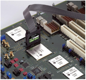
What does eMMC Interface look like?

eMMC,SD,SDIO

System Overview of eMMC Protocol

Communication Signals of the eMMC Protocol interface are as below

Clock: This signal is driven by the host controller to the device. Each cycle of this signal transfers one-bit command. But for data, it can be one bit or two bit depending upon the configuration. The frequency may vary from zero to maximum clock frequency specification. 

Data 0-7: There are eight data lines D0 to D7.  These are bi-directional data lines. It can either be driven by the host or the device. During the powerup or reset, only the D0 line is used for data transfer. A wider bus can be configured as 4-bit or 8-bit during the operation of the device. 

Data Strobe: This signal is generated by the device. Strobe is used for Data output and CRC status, response output in HS400.  The frequency of this signal follows the frequency of the clock. For data output for each cycle of this signal is two bits-one bit is for the positive edge and the other bit is the negative edge of the cycle. For CRC response status is latched only on the positive edge of this signal. 

CMD: This signal is a bidirectional channel used for device initialization and transfer of commands. Commands are sent eMMC Protocol host controller to the device and a response to these commands is sent by the device to the host in the CMD line.

RST: Hardware Reset

Vcc: Supply voltage for Core

Vccq: Supply voltage for I/O

Vss, Vssq: Ground for supply voltage core and I/O

eMMC Theory of Operations: eMMC Protocol Understanding 

eMMC Device set of information registers

Name Register Width (byte) Description
CID 16 Device Identification Number
RCA 2 Relative Device Address, is the Device system Address, dynamically assigned by the host during initialization
DSR 2 Driver State Register (Optional)
CSD 16 Device Specific Data, information about the device operation Condition
OCR 4 Operation Conditions Register. Used by the special broadcast command to identify the voltage type of the device
EXT_CSD 512 Extended Device Specific Data. Contains information about the device’s capabilities and selected modes.

After the power-on reset host needs to send a special message to the device to initialize the communication between the eMMC Protocol host and the device. This communication has three tokens command, response, and data token. A command token is issued by the host. A response token is issued by the device. Based on the command data can be either from the host or the device.

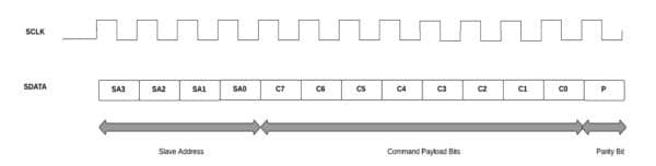
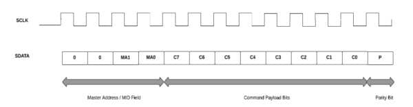
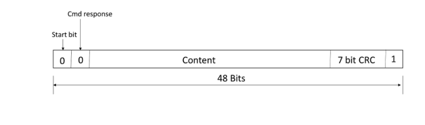
Command Token: Command is transferred from host to device. It is transferred serially on the command line. The command has the following bit coding scheme

eMMC,SD,SDIO

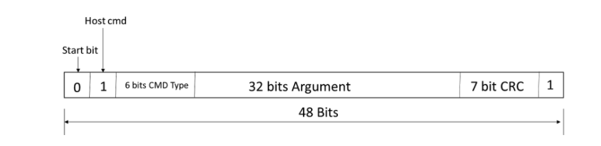
eMMC Protocol has 64 commands from cmd0 to cmd63. Some of these commands are reserved. Each command has a different function.

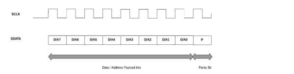
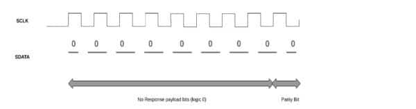
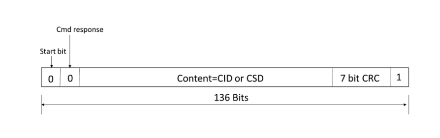
Response Token: This token is sent from the device to the host as a response to a previously received command. The response is serially transferred over the command line. The response has five coding schemes.  It could be either 48  or 136 bits. 48 bit wide responses are R1, R3, R4 and R5. R1’s response has card status information. R3 has OCR register information. R4 a dR5 has a relative card address. 136-bit wide response is R2. This has CID or CSD register information.

eMMC,SD,SDIO

R2 bit scheme is shown in this figure.

eMMC,SD,SDIO

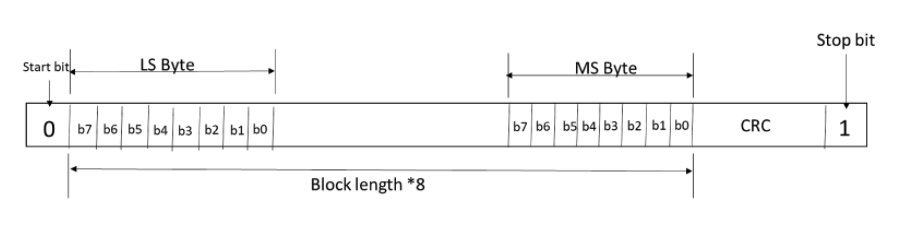
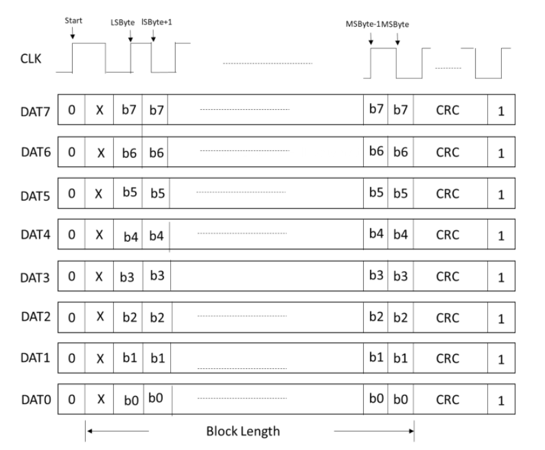
Data Token:  Data is transferred from the device to the host or vice versa. Data can be transferred in 1 line/4 line/8 lines using data lines. DAT0 is used for one line, DAT0-DAT3 is used for four lines, and DAT0-DAT7 is used for eight-line data transfer. For each clock cycle, either one-bit or two-bit (Dual/DDR) is transferred. One bit either is transferred at the rising edge and the second bit is transferred at the falling edge of the clock cycle.

One line DAT0 line coding 

Four-line DAT0-DAT3 line coding

eMMC,SD,SDIO

Eight-line DAT0-DAT7 line coding

eMMC,SD,SDIO

8-bit  DDR mode 

eMMC,SD,SDIO

Bus of Speed of eMMC Protocol System:  Bus speed is started with 25MHz SDR mode. Currently, the eMMC Protocol bus speed is 200MHz DDR mode. It is commonly known as HS400. The below table provides details of the different speeds of the eMMC Bus.

Mode Name Data Rate IO Voltage Bus Width Frequency Maximum Data Rate @bus width 8
Backward Compatibility with legacy MMC card Single 3/1.8/1.2V 1,4,8 0-26MHz 26MB/s
High Speed SDR Single 3/1.8/1.2V 1,4,8 0-52MHz 52MB/s
High Speed DDR Dual 3/1.8/1.2V 1,4,8 0-52Mhz 104MB/s
HS200 Single 1.8/1.2V 4,8 0-200MHz 200MB/s
HS400 Dual 1.8/1.2V 4,8 0-200MHz 400MB/s

eMMC Modes of Operation for Host and Device

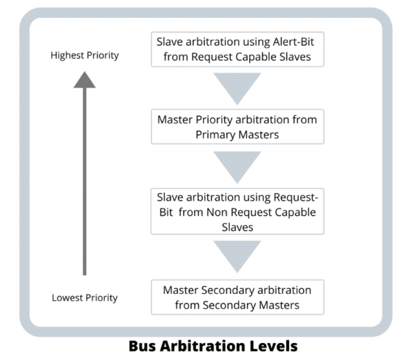
All communication between the host and the device is controlled by the Host. The host sends a command to the device resulting response from the device. There are five operation modes for eMMC System.

Boot Mode: The device will be in boot mode after the power cycle, reception of CMD0 with argument F0F0F0F), or assertion of the reset signal.

Device Identification Mode: The device will be in device identification mode after the boot mode or if the host and/or device don’t support boot mode. The device will be in this mode until the host issues the set RCA command CMD.

Interrupt Mode: Host and device enter interrupt mode simultaneously.  In this mode, there is no data transfer. The only message allowed is to interrupt service requests from either device or the host.

Data Transfer Mode: The device will enter the device transfer mode once RCA is assigned.  The host will enter the data transfer mode once it recognizes the device in the bus.

Inactive State: The device will enter inactive mode if either the device operating voltage range or access mode is not valid. The device can also enter inactive mode with the GO_INACTIVE_STATE command (CMD15). The device will reset to a Pre-idle state with a power cycle.

Debugging Protocol eMMC :

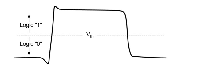
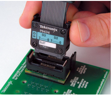
When working with eMMC, it is important to have the right set of tools to ensure the eMMC design is implemented properly. Having a protocol analyzer and oscilloscope is always helpful to debug complex hardware timing issues. 

An oscilloscope is helpful in case you want to measure the timing parameters of the eMMC Device.

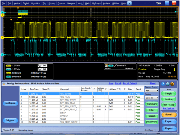
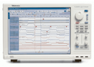
eMMC protocol analyzer can be very helpful to do eMMC packet sniffing. Prodigy Technovations also offers an eMMC trigger and decode software to debug your eMMC packets using a Tektronix oscilloscope.

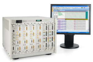
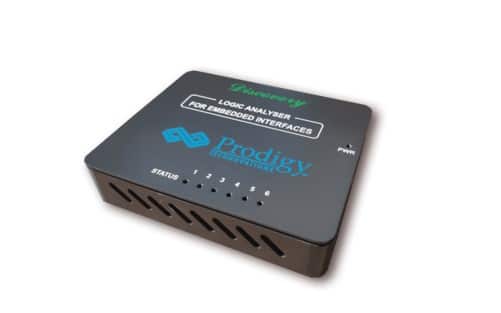
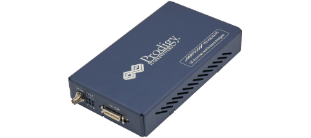
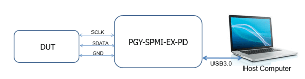
How does Prodigy Technovations Interfaces with eMMC Protocol?

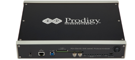
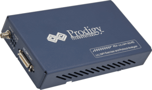
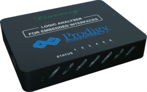
Prodigy Technovations has several different tools that interface with eMMC. The protocol analyzer is used to monitor the traffic that is happening on the bus. The eMMC protocol analyzer can capture the packets and help expedite debugging. This protocol analyzer can be used as an SD Protocol analyzer, SDIO protocol analyzer as well an eMMC protocol analyzer  

The product features are as follows:

  • Continuous monitoring of protocol data for a long time to capture elusive events (more than 30GB data capture)
  • Analysis of captured data per standards for protocol integrity, count of data bursts, CMD CRC errors, Response CRC errors, Data CRC errors, Timing Values, and Reserved commands
  • Hardware-based protocol-aware trigger capability in real time enables capturing specific Events. Triggering facility on patterns, commands, or error events.
  • User can identify the anomalies by decoding command and response arguments
  • Analytics feature provides analysis of acquired protocol data by plotting command, response, data, and frequency of operation over acquired time
  • Analytics feature also provides the decoding of device registers for easy analysis
  • Filters allow you to view specific packets in decoded protocol packets
  • Search feature for specific events in protocol activity
  • Easy-to-use user interfaces save time on the learning curve
  • Handles long-duration capture and displays the decoded data without demanding extensive resources in the host computer
  • Inserting markers [using Trigger-In] in protocol activity helps in correlating the input digital signal with Protocol Activity
  • Trigger-out signal for any specific protocol event allows triggering of other instruments such as oscilloscope
  • Interface to host system [running UI] using USB3.0 or Gigabit Ethernet interface
  • Flexibility to upgrade the hardware firmware using the GbE interface provides easy field up-gradation of firmware
  • Export of Decoded data packets to a Txt file for further analysis

eMMC-Protocol-Analyzer-1

SD, SDIO, eMMC Protocol Analyzer

Request For Quote

Share your requirement and our team will provide a tailored quote based on your validation needs.

"*" indicates required fields

This field is for validation purposes and should be left unchanged.
Address*

Request For Demo

Tell us your use case and our team will schedule a product demo aligned to your validation workflow.

"*" indicates required fields

This field is for validation purposes and should be left unchanged.
Address*

Request A Demo

Tell us your use case and our team will schedule a product demo aligned to your validation workflow.

"*" indicates required fields

This field is for validation purposes and should be left unchanged.
This field is hidden when viewing the form
Address*

Request Quote

Share your requirement and our team will provide a tailored quote based on your validation needs.

"*" indicates required fields

This field is for validation purposes and should be left unchanged.
Address*