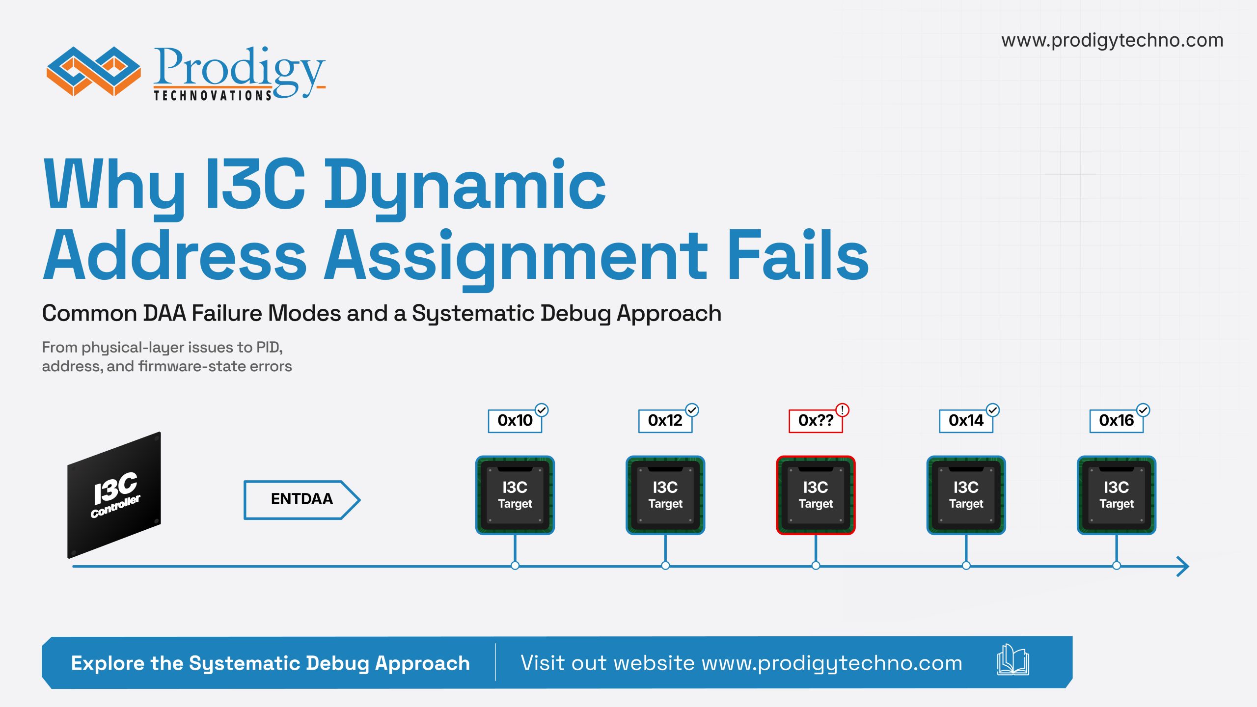
Dynamic Address Assignment, or DAA, the process by which an I3C controller assigns unique addresses to every device on the bus, is one of I3C’s most powerful features. It’s also one of the most common points of failure during bring-up. DAA is highly timing-sensitive and dependent on both protocol correctness and electrical integrity. A single issue can cause the entire sequence to fail. What makes these failures especially difficult to debug is that DAA failures are often silent. Devices may simply disappear from enumeration, fail to receive an address, or intermittently respond during bring-up, leaving engineers with little indication of where the breakdown actually occurred. Here, we’ll cover the most common DAA failures, how to systematically debug them, and what good visibility into the process actually looks like.

What Can Go Wrong During DAA

Infographic showing 8 common causes of I3C Dynamic Address Assignment (DAA) failure, including PID collision, invalid PID, I2C mode, chip readiness, and timing issues.

DAA failure in I3C? PID collisions, invalid PIDs, timing issues, and device readiness are some of the most common hidden causes. Identify them faster and simplify debugging.

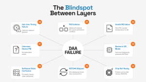
The I3C address assignment process often encounters lots of failures. And when it fails, the symptoms are rarely obvious. Here are the most common failure modes:

  • PID collision: If two identical chips share the same Instance ID, both transmit identical bits during arbitration. The controller assigns one address, and the second device becomes invisible.
  • Invalid PID value: Every I3C device’s 48-bit Provisioned ID must be non-zero. If it isn’t, ENTDAA will still assign a dynamic address. But any subsequent read or write transaction to that device will fail.
  • Device still in I2C mode: ENTDAA only works with devices operating in I3C mode. If a device hasn’t transitioned out of I2C mode, either because the bus frequency isn’t configured correctly or because the target’s I3C mode hasn’t been enabled as per its datasheet, it won’t respond to ENTDAA at all.
  • Chip not ready: A device may still be powering up or in a sleep state when ENTDAA arrives. The controller doesn’t flag this. It simply finishes DAA with fewer addresses assigned and moves on.
  • RSTDAA skipped: Devices holding addresses from a previous power cycle won’t participate in a new DAA sequence. They already have an address and ignore the request.
  • Software state confusion: RSTDAA clears hardware addresses, but if firmware doesn’t clear its internal tracking tables, the driver still assumes old addresses are valid. Any re-assignment gets blocked.
  • Device not in the known list: DAA assigns an address successfully, but the software has no descriptor for that device because its PID wasn’t registered in the device tree or firmware configuration.
  • Hot-Join timing problems: A Hot-Join device signals its presence after DAA has completed. If Hot-Join events aren’t enabled via ENEC or the interrupt handler is busy, the request gets ignored, and the device stays unaddressed.

Tools You Need to do I3C DAA Debug

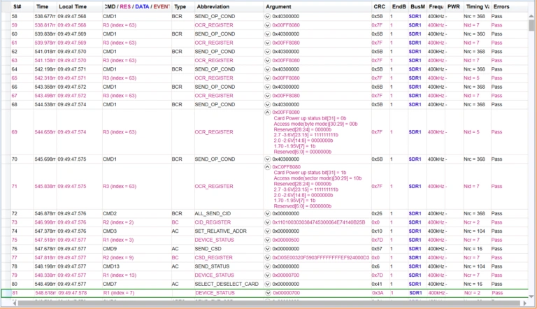
DAA debugging requires visibility at two levels, the physical signal and the protocol. These three tools cover both.

A Logic Analyzer

A logic analyzer shows you the digital signals on SCL and SDA decoded at the protocol level. For DAA debugging, this means you can see exactly what commands were sent, if the devices responded, what PIDs were transmitted, and whether addresses were correctly assigned.

An Oscilloscope

An oscilloscope shows you the actual analog waveform, which matters when the failure is physical.
Slow rise times, ringing on signal edges, or incorrect voltage levels won’t show up in a protocol decode. They only show up on a scope. If your logic analyzer shows a clean DAA sequence but devices still aren’t responding, the oscilloscope is where you look next.

A Protocol Analyzer and Exerciser

A dedicated I3C protocol analyzer actively participates on the bus.
In analyzer mode, it continuously sniffs all traffic, decodes every packet, timestamps every event, and flags protocol errors automatically. You see the entire DAA sequence laid out clearly like the PIDs received, addresses assigned, and ACKs and NACKs without manually interpreting waveforms.
In the exerciser mode, it can replace either side of the bus entirely. If you suspect your controller is mishandling ENTDAA, swap it out. Let the exerciser act as the controller and watch how your target devices respond. If you suspect a target device, do the opposite. This ability to isolate one side completely shortens a debug session by a lot.

How to Debug a DAA Failure

Infographic outlining a 7-step process to debug I3C DAA failures, including physical layer checks, ENTDAA verification, device response analysis, PID decoding, address validation, software inspection, and fault isolation.

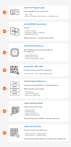
Follow this 7-step checklist to quickly diagnose and resolve I3C Dynamic Address Assignment (DAA) failures, from physical layer validation to software state analysis.

Work through these steps in order to systematically debug the I3C address assignment process:

Step 1: Check the physical layer first

Probe SCL and SDA with an oscilloscope before touching any software. Both lines should sit at VDD when idle. Look for slow rise times, ringing, or overshoot. If SDA is held low at idle, a device is stuck in a fault state. Fix this first.

Step 2: Diagnose the ENTDAA failure

Connect a protocol analyzer and trigger a DAA sequence, then confirm:

  • A START condition is generated
  • The broadcast address appears with a Write bit
  • The ENTDAA command code follows

If you don’t see this, the problem is on the controller side.

Step 3: Check whether devices are responding

After ENTDAA, at least one device should pull SDA low. If not, check whether RSTDAA was sent first, then confirm all devices are fully powered. And then verify bus voltage levels match your target devices’ expectations.

Step 4: Decode the PID transmission

Take note of the PID, BCR, and DCR fields and compare them against the datasheet values for your target device.
Corrupted bits or inconsistent values usually point to signal integrity problems rather than protocol errors. This is where it helps to correlate the protocol trace with oscilloscope waveforms.

Step 5: Count the assigned addresses

After DAA, count the number of addresses assigned and compare it to the number of I3C devices you expect on the bus. If the count is short, you likely have a PID collision or a device that failed to respond. Check your Instance ID configuration for all identical chips on the bus.

Step 6: Check the software state

Use verbose logging in your I3C driver and inspect:

  • Received PIDs
  • Address assignment status
  • Device descriptor initialization
  • Internal address tracking tables

If the driver still reports addresses as occupied after issuing RSTDAA, the most likely cause is a stale firmware state.

Step 7: Isolate the side that’s failing

If the root cause is still unclear, replace one side of the bus with a known-good reference.
Run ENTDAA from a protocol exerciser against your target devices. If enumeration succeeds, the controller implementation is likely at fault. Then reverse the setup. Replace the target side and observe how the controller behaves against a known-good device model. Incorrect behavior here points back to the controller stack.

How to Eliminate the Avoidable Failures

You can’t eliminate every DAA failure. Some like silicon bugs, PID collisions at scale, and intermittent signal integrity issues can still surface. But you can work to prevent the avoidable ones.

1. Always issue RSTDAA before ENTDAA

All of the bus initialization sequences must start with RSTDAA. Devices having addresses from a previous cycle won’t be able to participate in DAA.

2. Configure instance IDs for identical chips

If multiple units of the same chip share a bus, their Instance ID fields must be set to unique values. Check the datasheet and assign them deliberately before bring-up begins.

3. Clear software state when you clear hardware state

Engineers reset the hardware state, but might forget about the firmware’s internal address-tracking tables.
If RSTDAA clears device addresses on the bus while the driver still believes those addresses are occupied, the next DAA cycle can fail in confusing ways. Clear both sides together.

4. Register every device’s PID before bring-up

An incorrect entry can break the whole enumeration flow for that device in stacks that rely on pre-registered PIDs.
Double-check that each PID entry maps to the correct hardware on the bus.

When DAA Fails, Visibility is Everything

When DAA fails, you usually don’t get an error. The real problem, therefore, is the lack of visibility into the process.
Good visibility means different things at different layers.
In the physical layer, there has to be clarity on whether the signal edges are clean and voltage levels are correct. At the protocol layer, it means seeing every ENTDAA command, PID transmission, and address assignment in a single correlated view.
And when you need to isolate whether the failure is in your controller or your target, it means being able to replace one side of the bus entirely with a known-good reference and watching exactly what happens.
Prodigy Technovations’ PGY-I3C-EX-PD is built for exactly this. It combines a full protocol analyzer and exerciser in a single platform. It decodes every DAA transaction in real time, overlays protocol data directly on SCL and SDA waveforms, and flags errors automatically.
Its exerciser capability further simplifies root-cause analysis by allowing engineers to emulate either side of the bus using a known-good reference.
For electrical and timing validation, Prodigy’s oscilloscope-based I3C Electrical Validation Software complements protocol analysis with detailed signal integrity and compliance verification.
In the end, successful DAA debugging is about making the failure visible enough to understand, isolate, and fix with confidence. And Prodigy’s PGY-I3C-EX-PD provides the exact visibility engineers need. Find out what more it can do for your I3C bring-up process.

Today, the accelerated (32 GT/s) PCIe Gen 5 speed and the vast throughput of AI clusters dominate the technical vernacular in the modern data center. But a revolution is going on “beyond the main bus. The communication layer that monitors the health of the hardware, manages power states and protects hardware security is moving from legacy I2C/SMBus architectures to the Improved Inter-Integrated Circuit (I3C) standard. It’s partly due to the demand for deterministic, secure and fast telemetry in Compute Express Link (CXL) and DDR5 systems.

This discussion considers the reasons why SMBus cannot keep pace with the Legacy Wall

  • The I2C-based System Management Bus (SMBus) has been adequate enough for such simple tasks for years, such as accessing a voltage level or a temperature sensor. As systems have grown into AI fueled hyperscale systems, though, its shortcomings have become significant system-level constraints.
  • The number of buses in the bus loading problem and the complexity of the load multiplexer.
  • I2C’s top speed is 1Mbps. With high density components such as DDR5 modules that combine the SPD Hubs, PMICs and dual temperature sensors, the capacitance associated with these buses can sometimes make for the use of physical multiplexers (MUXes). This architecture brings in communication problems and boosts the possibility of signal integrity failures.
  • The Polling Tax
  • Unlike other bus types, in SMBus there is no efficient interrupt mechanism so the Baseboard Management Controller (BMC) dons the role of constant polling all of the devices. This results in the delay of response time and power wastage.
  • Fixed Addressing
  • Address is hardware bound in Legacy I2C. This becomes difficult in the case of a lot of identical devices in massive server racks which must be remapped to prevent collisions, otherwise it is not possible to address the databases.

The I3C Logic Stack (MCTP, SPDM and PLDM)

I3C addresses these problems with 12.5 MHz clocks to meet tight timing requirements, In-Band Interrupts (IBI) for signaling nearly instantaneously and Dynamic Address Assignment (DAA) that prevents static mapping conflicts. What is most significant is that it offers the strong transport services needed for contemporary management protocols.

  • MCTP (Management Component Transport Protocol) – It provides the framing for data transport for intercommunication between management controllers, GPUs, and CPUs, and their shared I3C bus, in a standard manner.
  • SPDM (Security Protocol and Data Model) – SPDM provides for the discovery, authentication and recovery of cryptographic measurement data from devices. A single SPDM transaction can take up to 100ms to complete a critical timing window during which if a bus hang or MUX induced glitch occurs, a secure boot sequence can be compromised or even become stuck (bricked).
  • PLDM (Platform Level Data Model) – PLDM is responsible for managing platform monitoring, platform power state change and firmware update throughout the platform to keep the system in a known, healthy state.

The sideband challenges in CXL and memory pooling

The sideband health is no longer “optional”, but necessary in CXL architectures to ensure memory coherency. In the event of a failure of the sideband bus (I3C/MCTP) during a memory-pooling request or during the retrieval of the security, the coherency or even the stability of the entire high speed AI cluster can be lost. Likewise, I3C is used in DDR5 and QSFP modules to overcome the problem of hundreds of sensors waking up at the same time, creating an initialization bottleneck.

What does it mean to validate? What is validation?

Tools that enable the validation of this sideband frontier need to enable more than just bit-level decoding – they must provide visibility and emulation on the protocol layer and system layer.

  • PGY-I3C-EX-PD Protocol Exerciser and Analyzer – Engineers can simulate Controllers, Secondary Controllers and Targets on this platform. It allows injecting CRC or parity errors in SPDM query-responses to test security-layer timeouts recovery by firmware.
  • Low-Cost Tooling – Solutions such as EX-PD-Lite are designed for manufacturing and Post-Silicon Validation (PPV) environments, while the I3C-USB Adaptor offers a light-weight, offline UI for field engineers to debug sensors when on the move.
  • For deep root cause analysis, protocol data needs to be correlated with physical layer waveforms, which is not possible with the Validation Alliance. Prodigy’s integration with high end oscilloscopes from Keysight, Tektronix, and LeCroy enables the engineer to go directly from an MCTP-packet error to the noise spike that arrives at the same location 5ns later.

Reliability of data centric is taking more and more to rely as well on integrity of sideband. Xorcom’s validation of the intent of sideband protocols, rather than packets, will continue to be a key distinguishing factor in high-performance engineering as industries transition to UFS 4.1 for automotive storage and CXL for disaggregated memory. Knowing how to use the I3C logic stack, validation teams can make sure that their designs are as fast and responsive as the high-speed buses they’re managing.

The change to the more modern Universal Flash Storage (UFS) 4.1 marks a turning point in the data architecture of mobile and automotive systems. The protocol can deliver on-device generative AI and advanced ADAS sensor fusion with rates of up to 23.2 Gbps per lane, or High-Speed Gear 5 (HS-G5) Rate B. This speed increase, however, poses a major “Signal Integrity Wall” for the validation engineer because the way it is observed can completely change the behaviour of the system under test.

The Physics of 23.2 Gbps and the Probing Crisis

Traditional passive interposers can be a low pass filter at the frequencies needed for HS-G5B, which can lead to the distortion of the M-PHY signal before it reaches the analyzer. The tolerance for these high-speed serial links becomes essentially zero; in fact, a few tens of picofarads of parasitic loading from a probe tip can “stub” the transmission line, generating false Cyclic Redundancy Check (CRC) errors and protocol “ghosts” not in the silicon itself.

To achieve true “Ground Truth” visibility at UniPro HS‑G5 speeds, validation must move to Active Probing. At 23.2 Gbps, UniPro/M‑PHY signals require substantial analog headroom, and only high‑bandwidth active probes can provide this while preserving DUT performance. Prodigy’s UFS active probes minimize electrical loading and maintain signal integrity, enabling the analyzer to capture the real timing of UniPro state‑machine transitions, including the High‑Speed Link Startup Sequence (HS‑LSS). This level of visibility allows engineers to identify and correct initialization inefficiencies, often reducing overall link‑bring‑up time by more than half.

In this session, students will learn about advanced Probing Architectures: mSMP and B2B Interposers

Among the most important physical issues of today’s device validation is the PCB density. Often there are not enough room for the regular SMPM connectors around UFS test points. The solution to this is two major high fidelity architectures that emerged,

  • Solder-down Active Probe Tips: These allow for direct access to M-PHY test pads between the host and the device. These tips provide high fidelity signal transmission with mSMP flexi-coax cables and are ideal for accessing the very close-packed mobile and automotive ECU boards.
  • Board-to-Board (B2B) Interposers: If the UFS device is not soldered to the main PCB, B2B interposers with embedded probe tips are a better option for development platforms. These interposers decrease the trace length between the test point and the analyzer’s front end, which minimizes the attenuation and reflections of the signal.

Demonstrating how protocol and physical layers are correlated.Validation Alliance: Correlating Protocol and Physical Layers

Decoding of protocols is no longer on its own. When it comes to deep root cause analysis, the engineers need to correlate a protocol-level event (like a Write Booster SLC cache flush) with the physical-layer events that generated it (like an HPB map correlation error).

The PGY‑UFS 4.0‑PA incorporates a dedicated Trigger‑Out SMA interface that provides deterministic, hardware‑level correlation between protocol‑layer events and physical‑layer signal behavior. The trigger engine inside the analyzer continuously monitors UniPro and UFS traffic for user‑defined conditions such as protocol errors, state‑machine anomalies, timing violations, or specific command sequences. When the configured event occurs, the analyzer asserts a clean, fixed‑width 100‑ns TTL pulse on the Trigger‑Out port. This pulse can be routed directly to a high‑bandwidth oscilloscope, enabling the scope to capture the exact analog waveform present at the moment of the protocol‑layer event.

The move from Consumer UFS 2.2 to Automotive UFS 4.1 is covered in this Strategic Roadmap

This Strategic Roadmap covers the move from Consumer UFS 2.2 to Automotive UFS 4.1.
A platform that can tie the entire storage roadmap together is required for validation maturity. UFS 4.1 is the standard of choice, but the performance/price ratio of UFS 2.2 is still ideal for many consumer consumer systems and automotive systems use UFS 3.1 for the challenging thermal conditions of the vehicle space where data storage must continue to perform reliably under temperatures ranging from -40 oC to +105 oC.

This 10-year evolutionary leap v2.1 – v4.1 needs to be covered by a modern validation tool on a single hardware unit. This means that “Backward Compatibility” doesn’t turn into “Behavioral Instability”, especially in transitioning between sleepy states (Hibernate) and “Zombie” power drains that can result from legacy firmware not exiting sleepy states during background flush cycles.

For flagship products, the ability to deliver peak theoretical performance won’t be the differentiator, it will be the ability to be “Day 180” reliable as we move forward with UFS 5.0 and beyond. With the probing paradigm and the use of high fidelity mSMP and B2B interposers, validation teams can break out of the synthetic benchmark. They can now see the truth of the protocol, making their designs communicate with purpose across all high-speed transitions.

The AI model is fine. The protocol stack down it is not.

The flaw of It Works in the Lab.

All of the on-device AI capabilities are verified during shipments. Face recognition gains straight off. The on-demand voice model is an immediate response. Real time camera processing is at full frame rate.

The stories from users three months later tell otherwise.

The AI feels “slower.” Face unlock constantly stops working. Life is not as promised by battery life. Users do not report that there was a particular failure. They complain of a feeling that the device is not as good as it was in the first day.

The AI model is not the root cause in practically every case that we have examined. It isn’t the NPU. The protocol stack is only the level that lies between the silicon and the data and the circumstance that no one tested it out in conditions similar to the ones it will be used in real life.

In this post, we discuss three common types of failures that can be observed in any mobile AI program: a storage protocol crash due to an AI workload, sensor bus crash due to thermal stress, and power management conflict due to concurrent AI workloads. Each one is preventable. All of them are not visible without the correct tools of visibility.

Failure Mode 1: UFS Storage Corrosion by Under AI Inference Load.

What the datasheet says

Write Booster paired with UFS 4.0 has a write speed up to 2,800 MB/s with a linear speed of 2,300 MB/s. Burst writes are absorbed by the SLC cache. The system is quick, energy-saving, and prepared to meet the requirements of the AI-workloads.

What actually happens

Write Booster is a performance gift that has a cost delay. The SLC cache is finite. User storage fills up to 6070 percent capacity which occurs over a few weeks with most users utilizing AI-intensive apps the company ware is forced to empty the cache back to TLC or QLC NA ND to clear the way to the next burst.

In that flush, three items get concurrent that do not appear in any datasheet benchmark –

The initial step to allow the data flow between the management and the internal data flow is that the M-PHY link goes into a management state. When loading model weights into a storage is happening to an AI inference task, the weight loads conflict with the flush to occupy link bandwidth. The NPU does not demand very hard, it only decelerates to a sluggish degree that the AI feature becomes slow. This spike of latency is not seen in a log file. It appears in a user review.

Second, when the UniPro Power Mode logic is not calibrated accurately, one would get a failure when the device enters the Hibernate mode in the case of flush cycles. The storage link remains half-active so that it has on power but does not do useful work. The consequence is destined validation engineers refer to as a zombie drain: a battery discharge rate that is 20–30 percent even greater than a spec guarantee, and is purely a result of a power state change that looks good when it is isolated but is ineffective when real combined workloads are involved.

Third, due to the SLC-to-TLC mapping fracturing with time the Host Performance Booster (HPB) mapping table becomes error-correlated. The HPB is created to speed up the performance of a random read by caching a map of commonly used logical block in host DRAM. By the time that map flakes apart, there are progressive increases in the latency of data fetching that make the previously AI-perceptive Day 1 feature seem visibly sluggish by Day 90.

None of this amounts to a hardware defect. That is all a foreseeable side effect of the Write Booster architecture in practice and that it is all completely avoidable should the validation team be in a position to view what is actually going on in the protocol layer.

What justification must embrace.

Write Booster under concurrent AI inference loads Write transition Write transitions under concurrent AI inference loads Not operated under only synthetic write benchmarks.

  • UniPro decode Power Mode when entering and leaving background flush cycles View of PACP indicates the link in a clean or partially suspended state.
  • Distribution of Latency range across the entire storage fill curve not peak latency, and not averages. The 99 th percentile at 70 percent fill during the load of the AI is the number which reflects what the user thinks they will perform at 6 months.

The PGY-UFS 4.0-PA is capable of giving M-PHY, UniPro, and UFS instantaneous cross-layer correlation over a single time-stamped view. In a configuration where a Write Booster command is chosen on the UFS layer, the software correlates automatically down to the state transition of the M-PHY that caused theWrite Booster command. Visually, engineers are able to determine whether the workload on AI inferences and the storage flush are interacting and precisely where the latency cost is being incurred.

Failure Mode 2 – I3C Sensor Security Under Thermal Stress.

The failure that is only experienced in the field.

I3C was created as a replacement of I2C due to the sensor-rich nature of the modern mobile devices that are currently providing faster speeds, less power consumption and in-band interrupts. In case of AI-driven capabilities that require the use of multiple sensors at the same time (face recognition, gesture detection, always-on camera), I3C is the bus which enables the architecture.

The bus is also the one that produces a category of failure that is extremely hard to replicate in a laboratory.

Dynamic Address Assignment (DAA) is the most insecure. Contrary to I2C, where addresses of the devices are determined during the design, I3C devices will allow their addresses to be determined on-the-fly each time the bus is reset. In a mobile device that wakes up in deep sleep the bus reset occurs in milliseconds and it occurs when the device may be in a different thermal state than when the device went to sleep.

Within one of the programs that we enabled, one out of every 12 units shipped would fail: a deep sleep cycle longer than 45 minutes later the ENTDAA (Enter Dynamic Address Assignment) sequence would not be responded to by one of three sensors attached to the I3C bus. As far as application processor is concerned, the sensor just was not there. The AI feature relying on the sensor in this instance, face unlock would not work without any notice.

The bench test environment was able to replicate the failure all 500 test cycles with no difference. The thermal recovery curve of an inactive device that spent 45 or more minutes in the pocket of a user just did not agree with a 5-minute idle cycle done by the lab work.

Once the correct thermal soak conditions were recreated and the I3C bus reset was recorded on the PGY-I3C-EX-PD throughout the ENTDAA sequence the failure could be observed right away: a 10µs timing window where the sensor was responding within the assignment of its address and yet not within the acceptance threshold of the master. The fix took 4 hours. It took 3 weeks to rediscover the failure condition.

What confirmation must have found?

  • DAA tests in realistic thermal operation conditions in particular, cold-soak, and extended idle conditions recreating the state of the device at the end of real user idle states, not only bench idle tests.
  • When there is a multi-sensor concurrent wake condition on in-band interruption (IBI) when multi-sensors are all trying to signify the master at the same time, arbitration decides which sensor is granted priority, and whether or not any sensor address allocation is missed.
  • Bus reset behaviour following long-term deep sleep the master-to-slave timing tolerance decreases with lower temperature and must be tested over the operating temperature range, not only at the typical room temperature Bus reset behaviour: This should be tested over the operating temperature range and not just at the standard room temperature.

Failure mode 3 – SPMI Power Arbitration Under Simultaneous AI Load.

The bus which links the Application Processor and the 5G Modem to the Power Management IC (PMIC) is the System Power Management Interface (SPMI). All Dynamic Voltage and Frequency Scaling (DVFS) events upon each NPU activation at inference task, each time the modem changes its power state when performing a 5G handoff is a SPMI-bus command.

One SPMI transaction is easy and quick all by itself. The SPMI bus is made a contested resource under mixed AI workload, modem activity and thermal management activities.

Its failure mode is arbitration deadlock: the CPU and the Modem are both commanding the same power-rail at the same time, and the arbitration logic in the firmware falters in resolving the conflict than the time the NPU would have taken to raise the power level. This leaves the brownout rather than the crash, but the inference task will fail with no notice or give incorrect results.

In the case of consumer AI features, this can be seen through the form of sporadic incorrect recognition outputs, the AI feature occasionally displaying stutters when running in real time, or the AI feature silently devolving to a lower-precision model without informing the user. These are intermittent failures that are thermal and load-specific and hardly ever repeatable at the bench without the specific combination of NPU load, modem activity and ambient temperature that causes the failures to occur in the field.

To prove the validity of SPMI power arbitration under AI workload it is necessary to observe the bus at the times of co-occurring NPU inference, modem 5G handoff and thermal management occurring. The PGY-SPMI-EX-PD offers microsecond-degree timing overview into the SPMI transactions, which enable engineers to see precisely how extensive a power command waits on the arbitrization queue before it is executed, and whether any NPU power ramp is being withheld because of modem priority traffic.

Why “3am” Is Not Just a Metaphor

This title of this post is not a disinvented one. The conditions of failure which are most significant in terms of on-device AI are the ones that happen not within a controlled environment: the phone that has been constantly running during a lengthy commute, the thermal situation that can only happen after 6 months of uncontrolled usage when the storage space is 72% full.

By definition, lab validation is unable to simulate all real-world conditions. However, it will be capable of simulating the state of failure that will be important when the validation team can see the protocol-layer and are aware of what to expect.

The three recovery scenarios presented in this post UFS storage breakdown due to AI inference load, I3C sensor bootstrapping due to thermal loading, and SPMI power arbitration due to identical AI workload are not conceptual. The three have been witnessed in all production programs. The three were all out of sight of tools used to monitor the system level. All that was evident in protocol-layer traced out when the right tools and conditions were involved.

On-board AI is no NPU problem only. Most of the risk is at the protocol stack and it is a system validation problem.

The implication of This on Validation Teams.

Three of the practical changes that would enhance AI feature validation coverage without making VC evaluation cycle substantially longer:

  • Test on real fill not empty store. Test the device storage with 6575% capacity of data storage. It is the mark where the Write Booster behaviour of flush starts becoming significant. The majority of validation laboratories operate equipment at 10-20% fill that is not reflective of the equipment condition 3 months into the actual operation.
  • Duration idle should equal actual user behaviour. There are thermal and time-dependent I3C DAA failures. A 5 minutes idle cycle at the bench does not mimic a 45 minutes pocket idle. Include additional idleness sequences to I3C validation test suite, which includes cold-soak, extended-idle, and thermal-stress conditions.
  • Arbitration SPMI must be validated with both combined load and not isolated transactions. The failures of SPMI with AI load only manifest themselves when NPU, modem and thermal management systems are at work. An SPMI validation with combined load, monitored with a timing resolution of µs, captures the arbitration conflicts which isolated testing does not capture at all.

The protocol stack below the AI chip is just as good as the AI chip itself. Validate the stack.

You have spent eighteen months on your new 5G flagship. Your RF department has adjusted your antennas to surgical accuracy. In laboratory, conditions controlled, the connection is an illusion. Yet there comes the truth, which is, the Carrier Certification. The hand-off fails. Band switching gives the throughput a precipitous fall. The connection is “live” though the rate of data is half of what was promised.

Checking the logs again, there is no issue with hardware failure, no broken element. You find a timing ghost. The simple RFFE bus in the 5G New Radio (NR) world has become a dangerous chokepoint where a couple of microseconds can mean the difference between the successful launch and multi-million dollar delay.

The Hidden Complexity of Carrier Aggregation

The shift to 5G is not only about increasing the speed of the technology, but it is more of a huge increase in the number of bands your device has to handle at the same time. Your modem is always playing a game of Carrier Aggregation to combine various frequencies to achieve maximum throughput to meet demand.

Whenever your device changed its band or has changed its antenna, it is MIPI RFFE bus that gets to do the heavy lifting. It screams on Low Noise Amplifiers (LNAs), Power Amplifiers (PAs), switches, and antenna tuners.

Complexity vs Determinism

The Problem

  • The larger the number of devices you connect to that common RFFE bus the greater you generate. In 5G NR, the spacing between subcarriers has become much less, so now your time to re-configure the RF front-end is limited dramatically.

The Penalty

  • Two microsecond late triggering Timed Trigger to an antenna tuner causes the modem to lose its phase lock. Your device simply disappeared in the blink of an eye to the carrier base station. The connection goes dead and your certification is left without hope.

The reason why Troubleshooting in a Textbook is a Trap

Software-level logs or simple protocol decoders are used a debugging technique done by most engineering teams when trying to debug these hand-off failures. This is a dangerous mistake.

A request-side truth that they tell you is software logs that the processor requested in sending a command. They do not provide you with the truth of the bus-side, of the nanosecond when the SCLK to SDATA transition was complete or the delay by which Slave took to respond to the command.

Unless you are measuring the Trigger-to-Execution latency on the hardware level, you are not debugging, you are guessing. You do not see the 2.5ns jitters, or the microsecond slipovers that literally put the system into a crash.

Reservation Your Budget of time back

These “war stories” have been enacted in the industry at Prodigy Technovations. Your carrier certification should not be a dice throw in our opinion.

We have our PGY-RFFE-EX-PD, which is geared towards placing you in complete control of the RFFE environment even before you ever enter the certification lab:

Precision Stress-Testing

  • You may insert timing delays into the bus in 2.5ns steps, you may take the role of the Master. You could deliberately cause your RFFE slaves to reach the limit of their capacity so that you can know where they start losing commands.

Back-to-Back Trigger Validation

  • Timed triggers in RFFE v3.0 enable close simultaneous reconfiguration of a range of components. The exerciser is simulating the modem traffic that is on the high speed to demonstrate that your hardware can support these fast trigger strings.

Cross-Domain Correlation

  • The software does not simply list the packets but will automatically correlate the protocol data with a raw timing view. In case of a microsecond slip in a band hand-off you can observe the red flag just at the position where the event occurred on the actual wire.

The Bottom Line

The fight against 5G is decided within the microseconds. Unless your RFFE bus is deterministic, then your 5G performance is a myth.Quit permitting timing ghosts to determine the achievement of your product. Make sure that the purpose of your RF design matches the accuracy that it warrants.

You have just thrown away a small fortune in Gen 5 server chips. The datasheet promised 32 GT/s. Your promotional staff are already trumpeting about record throughput. But in the rack? The performance is tanking. The work loads in your multitennants are slacking, and your Express Lane is beginning to resemble rush hour at the airport terminal. What is wrong with your high-speed silicon! And it is not a signal integrity problem. It’s a Protocol Logic crisis.

The “Arbitration” Trap

Gen 5 of PCIe provides you with a larger pipe, yet does not identify the user of the pipe. When your controller is trying to fetch benchmark numbers by optimizing enormous Bulk Writes it will probably be starving your high-priority Metadata.

The Reality

In the case of a offending bulk dump consuming the queue, your cloud SLAs are diluted by latency. You are not operating a data centre, you are operating a bottleneck.

Ghost in the Machine – LTSSM Recovery

At 32 GT/s, heat is your enemy. Connections to your server rack warm up, your connection may be imperceptibly degenerating into an LTSSM (Link Training and Status State Machine) state of Recovery.

Credit starvation (The Silent Killers of performance)

When your receiver is unable to clear its buffer at a pace faster than the Flow Control Credit is being issued, it will cease to issue the Flow Control Credits.

The Problem

Instead of crashing, the system is slowed down to restart training sequences. To the architect, it’s a “ghost.” To the user, it’s a laggy server. An oscilloscope can never do this.

The Result

The transmitter just. stops. When your 32GT/s connection is being used, it is actually reduced to Gen 3 speeds since the protocol is waiting the clear to send signal which is not received.

The Bottom Line

Stop selling your data center as a black box. When you only certify the physical pipe, you are half the truth. We help you find the why at Prodigy Technovations. Our PGY-PCIe Gen3/4/5 Protocol Analyzer provides deep NVMe 2.0 decoding, detailed LTSSM state machine transitions for both upstream and downstream links, and comprehensive sideband signal decoding. This enables you to clearly demonstrate that your silicon is performing all the functions promised in the datasheet. Stop chasing benchmarks. Start validating intent.

The amount of pressure to reduce the weight of wiring is extreme in the migration to Zonal Architectures and Software-Defined Vehicles (SDV). It has caused a significant architectural change that has concentrated high-speed Automotive Ethernet backbones as a form of consolidation in order to support both non-critical and infotainment data and safety-critical ADAS traffic.

This is on paper, an efficiency victory. It is a high stakes trade off in the lab that puts Quality of Service (QoS) and system isolation to the test.

Convenience vs Determinism

The key issue facing architects of the modern automotive is ensuring that the failure in one non-critical system starts to bleed into a safety-critical one.

  • The Intent – Use one and high-speed 100BASE-T1 bus and manage both certainly the streams of Spotify and the alarm in the emergency braking car.
  • Risk – When the PTP (Precision Time Protocol) synchronization fails or in case of a burst of infotainment traffic leading to overflow of a buffer, the determinism of the safety-critical system is lost.

The Reality of Engineering – The Isolation Is Not Easy

Hardware failure is not the most dangerous type of crash, it is Priority Inversion.

  • We have seen the situation when a basic door controller on a CAN-FD bus has begun generating Error Frames because the checksum in its response matched a mismatch. This may take up the processing bandwidth of the Gateway ECU causing the delay of important safety packets.
  • A crashing information entertainment system is an inconvenience. The infotainment system with a delay in the backup camera screen feed is a regulatory breach according to the ISO 26262.

Visibility is the Antidote

In Prodigy Technovations, we think that you are not supposed to make any guess on whether or not your safety-related traffic is secure. These architectural boundaries are tested by our Automotive Suite. 

  • Zero latency passive Tapping – The PGY-100BASE-T1-PA is based on passive tap solution. This guarantee the ground truth of the bus timing without necessarily introducing to the network by the analyzer an extra microsecond of latency.
  • Multi-Bus Simultaneous Correlation – CAN-FD, LIN and Ethernet can all be checked using the PGY-LA-EMBD at the same time. This will enable you to observe what point on a slow bus causes a glitch on the high speed backbone resulting in a timeout.
  • High-Resolution Timing High 1GS/s timing – We assist you in capturing the noise spikes of 5ns that are absolutely impossible to record using a standard software.

Good engineering is concerned with fewer mistakes. Do not turn a compacted architecture into a point of destruction.

In the mobile industry, “Day 1” performance is easy to promote. But true engineering skill shows in “Day 180” performance. When a flagship device feels “laggy” after six months of real use, it’s rarely the processor’s fault. Usually, it’s a trade-off problem in the storage layer, especially how the system handles Single Level Cell (SLC) cache flushing and its effect on the protocol stack.

Marketing Bursts vs. Architectural Sanity

To achieve the fast sequential write speeds that help sell devices, UFS 4.0 uses Write Booster logic to store data in a high-speed SLC buffer. The challenge comes when this buffer fills up. To keep performance steady for the next burst, the firmware has to move, or flush, that data to the higher-density TLC or QLC NAND.

This presents a critical choice for Architects that impacts the entire protocol layer:

  • Background Flushing: To keep the cache free for the subsequent burst, the system initiates a flush right away. However, when 8K video is being recorded or when an app is launching quickly, these background actions compete with foreground user duties, resulting in abrupt latency spikes.
  • Idle-Time Flushing: The system waits for the device to be inactive. But if the UniPro Power Mode logic isn’t perfectly calibrated, the device may fail to enter deep sleep states correctly during the flush. This causes a “zombie” power drain that ruins battery benchmarks.

Validating the “Silent Killers” of Performance

We believe the role of a protocol analyzer isn’t just to see packets, it’s to provide the technical evidence needed to validate these high-stakes trade-offs. When a device fills to 70% capacity, fragmentation and cache management issues become the “silent killers” of user experience.

To ship a device that feels as fast at six months as it did on day one, validation teams must move beyond “max speed” and observe real-world behavior:

  • Layer Correlation: The PGY-UFS 4.0-PA provides instantaneous decoding and correlation across MPHY, UniPro, and UFS layers. This allows engineers to see exactly how a UFS-level Write Booster command triggers MPHY state changes (like Stall or Prepare) in a single, time-stamped view.

Correlated MPHY, UniPro, and UFS layer analysis revealing real-time protocol behavior during cache flushing and command execution.

Time-correlated MPHY, UniPro, and UFS protocol analysis revealing how write bursts and cache flushing impact latency and link power states.

  • Long-Duration Stress Testing: Since cache issues are often time-dependent, the analyzer supports continuous streaming of protocol data directly to the host SSD. This enables teams to capture and analyze gigabytes of traffic over extended periods to catch the elusive 1% of latency spikes that occur during heavy flushing cycles.
  • Power State Transparency: The software features a dedicated PACP (PHY Adapter Layer Control Protocol) view, making it easy to analyze power mode change packets and ensure the link is transitioning between high-speed and low-power gears without “hanging”.

Good engineering is about making fewer wrong decisions. By utilizing a Floating Window architecture, architects can view UFS, UniPro, and MPHY views on separate monitors simultaneously. This visibility ensures that when a packet is selected in the UFS layer, it is automatically correlated down to the MPHY layer, revealing the hidden cost of every flushing decision.

Don’t let a hidden buffer flush kill your brand’s reputation. Use high-fidelity protocol evidence to ensure your “Day 180” performance matches the “Day 1” hype​.

xSPI vs OSPI

Introduction
In embedded systems and high-speed communication, xSPI (eXtended Serial Peripheral Interface) and OSPI (Octal Serial Peripheral Interface) are two popular protocols for interfacing with flash memory and other peripherals. While both are designed to improve data throughput over traditional SPI, they differ in architecture, speed, and implementation.

Feature Comparison

Feature xSPI OSPI
Bus Width Supports multiple data lines, typically 1, 2, 4, and up to 8 lines Uses 8 data lines for maximum throughput
Speed Can achieve high speeds depending on implementation Optimized for very high speeds, often >200MB/s
Complexity Flexible but may require more configuration More straightforward but hardware dependent
Use Cases General-purpose high-speed communication High-performance flash memory operations
Compatibility Backwards compatible with SPI and QSPI Primarily focused on octal memory devices

Conclusion
Both xSPI and OSPI are powerful interfaces for high-speed communication in embedded systems. xSPI offers flexibility and compatibility, while OSPI delivers unmatched throughput for octal memory devices. The choice between them depends on the specific requirements of the application, including speed, compatibility, and hardware support. New to xSPI and want to understand its features, advantages, and applications in depth?

Explore our full guide: Understanding xSPI  The Future of High-Speed Flash Memory Interfaces.

Debugging eMMC Boot Failures: Capturing & Analyzing Boot Data with PGY-SSM

Embedded systems rely on a flawless boot sequence from their eMMC storage to load firmware and hand off control to application code. Yet misconfigured partitions, corrupted boot data, or unexpected eMMC responses can derail this process, leading to silent failures that are difficult to diagnose with standard tools.
With the PGY-SSM SD/SDIO/eMMC Protocol Analyzer, you can capture the entire boot interaction in real time, pinpoint exactly where things go wrong, and visualize key protocol events all without interrupting the device under test.

Why eMMC Boot Failures Are Hard to Debug
  • Low-level communication: The boot process uses a series of commands (CMD0, CMD1, CMD6, CMD16, CMD17, etc.) and register exchanges (CSD, CID, EXT_CSD) before any filesystem is mounted.
eMMC Boot
  • Transient errors: A single erroneous response or CRC failure early in the boot sequence can prevent firmware from loading, but standard logic analyzers often miss these fleeting mis-transactions.
  • Complex modes: Modern eMMC devices switch between modes (HS400, DDR52, HS200) during boot. Verifying correct initialization requires both timing and content validation.
Key Capabilities of PGY-SSM for Boot Debugging
  • Continuous, long-duration capture (up to 30 GB): Never miss an elusive boot event, even if the failure occurs after repeated reset cycles .
  • Protocol-aware triggers: Set simple or sequential triggers on specific commands, responses or CRC errors (e.g., trigger on CMD1 with a wrong OCR response) to isolate the exact failure point .
  • Real-time Boot Data decoding: View decoded boot-partition commands and register reads (CSD, CID, EXT_CSD) as they happen, without manual post-processing .
PGY-SSM Boot Debugging
  • Boot-sequence selection: Configure the analyzer to also include boot data as sent by the device on power up.
  • Analytics Dashboard: Visualize command frequency, response times, and error counts over the capture period spotting anomalous patterns that point to configuration or timing issues .
Workflow: Capturing & Analyzing eMMC Boot Data
  • Setup & Boot-Mode Selection
  • Launch the PGY-SSM software and select Live Capture.
  • Under Current Target Settings, set Card Type to eMMC and enable Boot Sequence mode .
  • Choose the probe type and connect CLK, CMD, D0–D7 (and strobe for eMMC 5.x) to the analyzer.
Configure Triggers
  • Use Simple Trigger to catch a specific boot command (e.g., CMD1).
  • For deeper analysis, choose Sequential Trigger: for example, trigger on CMD0 → CMD1 → CMD6 to detect exactly which step fails .
Run & Capture
  • Click RUN. The analyzer streams all protocol activity to the host PC’s disk, capturing both commands and data bursts continuously .
  • If the failure occurs, the trigger starts capture at the precise moment—no need to sift through hours of idle traffic.
Live Decoding & Inspection
  • As data arrives, the Analyze panel shows a time-stamped, color-coded decode listing.
  • Drill into any packet to inspect arguments, CRC status, and register contents.
Analytics & Visualization
  • Switch to the Analytics view to see histograms of command indices, response latencies, and any CRC-error spikes across the boot sequence.
  • Identify outliers such as repeated busy-time spikes on CMD17 that may indicate device timing mismatches.
Report Generation
  • Export a CSV report of the entire boot session (with optional data inclusion) for offline review or sharing with firmware teams .
Real-World Impact
Real-World Impact

By combining deep protocol-aware triggers, real-time decoding, and long-duration capture, the PGY-SSM empowers engineers to:

  • Quickly isolate the exact phase where boot initialization fails whether it’s a misread EXT_CSD field or a CRC error on the initial CMD0.
  • Validate mode switches (e.g., entering HS400) by comparing actual register values against expected JEDEC specs.
    Accelerate firmware debug by providing crystal-clear protocol logs, eliminating guesswork.
Conclusion

Debugging eMMC boot failures no longer has to be a shot in the dark. With PGY-SSM’s targeted capture, powerful triggers, and intuitive analytics, you can trace every boot-phase transaction in real time and get your embedded system up and running with confidence.

Discover more about how PGY-SSM can streamline your eMMC validation and debug workflow at
prodigytechno.com/device/emmc-protocol-analyzer

Request For Quote

Share your requirement and our team will provide a tailored quote based on your validation needs.

"*" indicates required fields

This field is for validation purposes and should be left unchanged.
Address*

Request For Demo

Tell us your use case and our team will schedule a product demo aligned to your validation workflow.

"*" indicates required fields

This field is for validation purposes and should be left unchanged.
Address*

Request A Demo

Tell us your use case and our team will schedule a product demo aligned to your validation workflow.

"*" indicates required fields

This field is for validation purposes and should be left unchanged.
This field is hidden when viewing the form
Address*

Request Quote

Share your requirement and our team will provide a tailored quote based on your validation needs.

"*" indicates required fields

This field is for validation purposes and should be left unchanged.
Address*