Understanding xSPI: The Future of High-Speed Flash Memory Interfaces

Introduction to XSPI (What is XSPI?)

xSPI stands for “eXpanded Serial Peripheral Interface”. It’s a high-speed communication protocol designed to interface with NOR flash memory and other peripherals. xSPI is an enhanced version of the standard SPI, offering faster data transfer speeds and greater efficiency. xSPI supports multiple data lanes, which enables faster read and write speeds compared to the traditional SPI protocol. It is standardized under JEDEC JESD251 and JESD251-1.

Visuals:

Block diagram of xSPI Host (controller) connected to flash memory (Target) with arrows showing Clock, Chip select and multiple data lanes,

Why is xSPI important?

  • The increasing demand for faster data processing, such as in embedded systems, IoT (Internet of Things) and automotive electronics products has made xSPI crucial. It provides significant improvements in memory access speed, enabling faster boot times, quicker data retrieval, and overall enhanced system performance.

High-Speed Data Transfer

  • Supports Octal SPI (8-bit wide) for faster communication.
  • Offers speeds up to 400 MB/s or more with DDR (Double Data Rate) mode.

Improved System Performance

  • Reduces boot time for embedded systems.
  • Efficient memory-mapped read access for processors, enabling seamless execution of code from external flash.

Standardization and Interoperability

  • Ensures compatibility across different flash memory vendors.
  • Simplifies the integration process for system designers.

Low Power Consumption

  • Optimized for battery-powered applications like IoT devices, automotive systems, and mobile devices.

Advanced Features

  • Error Correction Code (ECC) for improved data integrity.
  • Security features like authentication and encryption for secure boot and firmware updates.

What is the advantages of xSPI over QSPI

  • Faster Data Transfer
    xSPI supports more data lanes than QSPI, which allows it to transfer data at higher speeds. This results in faster performance for systems that need quick data access.
  • Lower Latency
    XSPI reduces delays in data transmission, making it ideal for real-time applications where every millisecond counts, such as in automotive and industrial systems.
  • Greater Scalability
    xSPI can handle multiple lanes and is more flexible, allowing it to support higher speeds as technology advances, making it future-proof for growing data needs.
  • Better Performance in Complex Systems                                                                                                              xSPI is better suited for high-performance applications, such as high-resolution video or advanced sensors, where large amounts of data need to be processed quickly.
  • Improved Efficiency
    xSPI reduces bottlenecks in data transfer, allowing the system to operate more efficiently, leading to smoother performance in demanding environments.
  • Comparison of Traditional SPI, QSPI and xSPI

Frame format of SPI, QSPI and xSPI

  • SPI

  • QSPI

xSPI

1S-1S-1S Mode

8D-8D-8D Mode

Applications of xSPI

  • Automotive Electronics (ADAS, Infotainment, ECU firmware storage)
    Industrial Automation (real-time controllers, PLCs)
  • Aerospace & Defence (secure and high-reliability memory solutions)
  • Embedded Systems (MCUs, FPGAs, and SoCs requiring fast external memory access)

Looking to analyze and debug xSPI interfaces efficiently? The PGY-STG-PA XSPI Protocol Exerciser & Analyzer offers comprehensive testing capabilities with:

  • Support for xSPI/OSPI Protocols
  • Switching between 1SDR, 8SDR & 8DDR modes
  •  Single, Dual, Quad & Octal SPI compatibility
  • 8GB DDR memory for deep data analysis
  • Up to 8 IF-ELSE trigger levels for precise event capture

Explore how PGY-STG-PA can streamline your testing process. Learn more: https://www.prodigytechno.com/xspi-protocol-analyzer

Sideband Signal Analysis for PCIe Interfaces Using PGY-PCIeLP-SBA

Silicon vendors need to validate the electrical timing measurements of side band signals at different state of the DUT and see the consistency over long period of time.

To address this requirement Prodigy Technovations has developed PGY-PCIeLP-SBA PCIe Side Band Signal Analyzer. Which monitors these signals and gives the statistical information of the measurements over multicycle operation to ensure stable and reliable operation. The PGY-PCIeLP-SBA includes discovery series logic analyzer (palmtop size) with customized logic for PCIe Side Band signal analysis with REFCLK, Software to view the results and debug capabilities, flying lead probes with M.2 extender board with access to side band signals.

PGY-PCIeLP-SBA monitors CLKREQ, REFCLK, PERSET and PWR signals of the M.2 interface during the different operating conditions. It provides timing measurement of these signals as per PCIe and M.2 interface specification documents. User can also set hardware-based trigger on specific timing measurement failure and get notified. API supports the user test the DUT over a long period of time. User interface displays timing diagram with abstract view of the 100MHz REFCLK condition the low power state, restart and power recycle and power on state of the during while running the test case.

The typical test setup for PCIe Side band Signal analysis is:

pcie_sba_set_up

PGY-PCIeLP-SBA has M.2 extender board with access to all side band signals which can be connected to PCIe Low Power Side Band Signal Analyzer. The software runs in windows PC enables the configuration of Analyzer for measurements and trigger conditions. It continuously plots the timing waveforms and updates timing measurements summary statistical and detail information

Software will automatically detect the power on test, low power entry and exit test, restart test and sudden power shutdown test. It will make applicable measurements all these test cases and reports the results in listing form. It will also provide statistical information of the timing measurements and continuous plot of timing diagram of the side band signals.
User can correlate any specific timing measurements in the measurements detail listing view to the timing waveform plot to locate this event.

User can sort the pass or fail results in the listing view. If any specific timing measurement needs to corelated to the timing waveform which has entire data of all test cases, user clicking the timing measurements locate this in timing waveform.
For efficient method to capture the elusive events PGY-PCIeLP-SBA provides trigger on timing measurement failure. The pre and post trigger data enables the user to view the data prior to trigger event and post trigger event to identify the probable cause to the timing failure. The trigger and corelating the timing measurement to timing diagrams make it a efficient debugging tool.

PGY-PCIeLP-SBA PCIe Sideband Signal Analyzer is the industry first portable instrument with software which can analyzer the sideband signals during different state of the PCIe interface. The Discovery logic analyzer which is included in PGY-PCIeLP-SBA also support trigger and protocol decode of I3C and I2C (SM Bus) interfaces. This makes it most complete low cost easy to use instrument for any design, pre and post silicon test and field engineers to validate and debug the side band signals.

Want to learn more? Join our webinar on “Overview of PCIe Sideband Signal Functionality at Power-On & Low Power State, and Validation.”

Register here: https://www.prodigytechno.com/overview-of-pcie-side-band-signals-functionalities-at-power-on-low-power-state-and-validation

Prodigy Technovations offers a PCIe Low Power Side Band Signal Analyzer to help you capture and analyze critical signal behavior during power transitions.
Learn more: https://www.prodigytechno.com/device/pcie-low-power-side-band-signal-analyzer

PCIe Sideband signal operation during lower Power entry and exit

In modern applications such as mobile devices, servers, gaming systems, and network storage, there is a growing demand for increased storage capacity. To meet this need, many of these devices are transitioning to solid-state drives (SSDs) using the NVMe protocol over PCIe. While PCIe has traditionally been considered a power-hungry interface, the PCI-SIG (PCI Special Interest Group) has been continuously evolving the PCIe specification to enhance performance while reducing power consumption, especially to support emerging, power-sensitive applications.

For battery-operated devices, it is critical to achieve fast wake-up times and longer battery life without fully powering down the device. Additionally, when the PCIe interface is idle, it must consume minimal power and be able to return to an active state seamlessly, without degrading the user experience.
To address these requirements, PCI-SIG introduced L1 Substates (L1.1 and L1.2) as part of the PCIe power management architecture. These substates leverage the existing CLKREQ# signal, which is extended to support additional signaling for power control. This allows PCIe transceivers to power down their high-speed circuits during inactivity and use CLKREQ# to wake them up when needed.

With L1 Substates, power consumption can be reduced dramatically—from approximately 400–500 mW in the active L0 state to just 2–3 mW in L1.2, enabling significant power savings while maintaining responsiveness.

pcie

To ensure the interoperability between different root complex and end points the timing between to CLKREQ and REFCLK needs to be maintained. PCI-SIG recommends the timing values are

pcie

Power-Up CLKREQ# Timings

Symbol

Parameter

Min

Max

Units

Note

TCRHoff

CLKREQ# de-asserted high to clock parked

 0


 ns

TCRLon

CLKREQ# asserted low to clock active


400

ns

See note

Note: TCRLon is allowed to exceed this value when LTR is supported and enabled for the device.The Latency Tolerance Reporting (LTR) mechanism allows a device to inform the host (Root Complex) about how long it can tolerate delays before its requests (such as interrupts or memory accesses) must be serviced. This helps the host coordinate power management and efficiently schedule servicing across multiple devices without compromising performance. LTR information is exchanged during the PCIe link-up phase, as part of the configuration and training sequence, allowing the host to make informed decisions on entering low-power states while still meeting device latency requirements.

Want to learn more? Join our webinar on “Overview of PCIe Sideband Signal Functionality at Power-On & Low Power State, and Validation.”

Register here: https://www.prodigytechno.com/overview-of-pcie-side-band-signals-functionalities-at-power-on-low-power-state-and-validation

Prodigy Technovations offers a PCIe Low Power Side Band Signal Analyzer to help you capture and analyze critical signal behavior during power transitions.
Learn more: https://www.prodigytechno.com/device/pcie-low-power-side-band-signal-analyzer

During the power-on sequence of a PCI Express (PCIe) system, the reference clock (REFCLK) and sideband signals may not have reached their required stability or operating tolerance. The PERST# (PCIe Reset) signal is an active-low, open-drain output driven by the Root Complex (RC). It is used to hold the endpoint (EP) devices in reset while the system’s power and clock signals stabilize.

The PERST# signal remains asserted (held low) until the RC confirms that the power rails and REFCLK are stable. Once these are within specification, the RC deasserts (releases) PERST#, signaling to endpoint devices that the system is ready to begin PCIe link initialization.

pcie_sideBand_signal
The timing diagram shows the usage of PERST Signals

From the endpoint’s perspective, the deassertion of PERST# acts as a global reset release and indicates that power and clocks are valid, allowing the endpoint to start its PCIe link training and initialization process.
To ensure successful link initialization and operation between the Root Complex (RC) and Endpoints (EPs), the following timing requirements must be observed:

Symbol

Parameter

Min

Max

Units

Note

TPVPGL

Power Valid to PERST# input inactive

Note 1


ms

2

TPERST#-CLK

REFCLK stable before PERST# de-assertion

100


µs


TFAIL

Power level invalid to PERST# assertion


500

ns


TPERST

Assertion time of PERST#

100


TPERSTSLEW

Slew rate of PERST# transition to de-asserted

50


mV/ns

3

Want to learn more? Join our webinar on “Overview of PCIe Sideband Signal Functionality at Power-On & Low Power State, and Validation.”

Register here: https://www.prodigytechno.com/overview-of-pcie-side-band-signals-functionalities-at-power-on-low-power-state-and-validation

Prodigy Technovations offers a PCIe Low Power Side Band Signal Analyzer to help you capture and analyze critical signal behavior during power transitions.
Learn more: https://www.prodigytechno.com/device/pcie-low-power-side-band-signal-analyzer

UFS 4.0 in Automotive: Powering Next-Generation Vehicles

In today’s rapidly evolving automotive landscape, vehicles are transforming into sophisticated, connected computing platforms. As manufacturers push the boundaries of safety, connectivity, and user experience, the need for high-performance storage solutions becomes paramount. Universal Flash Storage (UFS) 4.0 is emerging as a critical technology that meets these demands, offering ultra-fast data transfer, low latency, and improved energy efficiency. In this post, we explore how UFS 4.0 is revolutionizing automotive systems and why it is becoming the backbone of next-generation vehicles.

The Need for High-Performance Storage in Modern Vehicles

Automotive systems are no longer limited to simple control functions; they now encompass advanced driver assistance systems (ADAS), immersive infotainment, real-time telematics, and even autonomous driving capabilities. These applications require rapid access to vast amounts of data from high-resolution sensor feeds to complex multimedia content. UFS 4.0, with its impressive interface speeds (up to 46.64 Gbps per storage device), significantly outperforms older storage solutions like eMMC, ensuring that critical data is available when it’s needed most.

Key Benefits:
High-Speed Data Transfer:

UFS 4.0 delivers ultra-fast read and write speeds, enabling quicker system boot times and rapid application loading. This is essential for infotainment systems that rely on seamless multimedia playback and for ADAS systems that must process sensor data in real time.

Support for Autonomous Driving:

Autonomous vehicles depend on a continuous stream of data from cameras, radar, and LiDAR sensors. UFS 4.0’s high-speed transfer capabilities ensure that this information is processed swiftly, supporting real-time decision-making that is crucial for collision avoidance and lane departure warnings.

Enhanced User Experience:

Modern infotainment systems demand high-capacity storage for maps, apps, and media. UFS 4.0 provides the speed and capacity needed for smooth, responsive interfaces, ensuring that drivers and passengers enjoy a superior in-car experience.

Energy Efficiency:

In an era where electric vehicles (EVs) and hybrid systems are on the rise, energy efficiency is critical. UFS 4.0 consumes less power compared to older flash memory types, helping to extend battery life without compromising on performance.

Reliability and Security:

UFS 4.0 is designed to operate reliably under the demanding conditions of automotive environments, including temperature extremes and mechanical vibrations. Its advanced security features, such as inline encryption, further ensure that sensitive data remains protected against cyber threats.

Real-World Impact: Enhancing Automotive Systems

The integration of UFS 4.0 into automotive systems is not just about faster storage it’s about enabling a host of advanced applications:

For ADAS and Autonomous Driving:

Fast and reliable storage allows for the rapid processing of sensor data, enabling systems to make split-second decisions that enhance road safety.

For Infotainment and Telematics:

High-speed storage supports rich multimedia experiences and real-time navigation, improving both the driving experience and overall vehicle connectivity.

For Future-Proofing Automotive Systems:
As vehicles become increasingly software-driven, the need for scalable and robust storage solutions grows. UFS 4.0 provides a future-ready platform that can accommodate evolving requirements without compromising on performance.
Conclusion

Universal Flash Storage 4.0 is set to become a cornerstone of next-generation automotive technology. Its ability to deliver fast, reliable, and energy-efficient data storage meets the high demands of modern vehicles, from advanced safety systems to cutting-edge infotainment. As the automotive industry continues to innovate, UFS 4.0 will play an essential role in shaping the future of connected, smart vehicles.

Prodigy Technovations offers industry-leading solutions for UFS validation and testing, including the PGY-UFS4.0-PA Protocol Analyzer, SoC-based UFS Tester, and UFS Protocol Decode Software. These tools empower engineers to analyze, debug, and optimize UFS communication in automotive systems.

Understanding Clock Stretching in I²C Communication and How PGY-I2C-EX-PD Simplifies Debugging

Efficient communication between devices is crucial in modern embedded systems, especially when using protocols like I²C (Inter-Integrated Circuit). One of the key mechanisms that ensures smooth data transfer between fast masters and slower slaves is clock stretching. This blog explores the importance of clock stretching, the challenges engineers face, and how the PGY-I2C-EX-PD tool provides effective solutions.

What is Clock Stretching and Why Is It Important?

In I²C communication, the master device generates a clock signal to synchronize data exchange with slave devices. However, some slave devices may require additional time to process data or respond to commands. Clock stretching allows these slower slaves to hold the clock line low temporarily, pausing communication until they are ready. This mechanism prevents errors such as missed data or corrupted transmissions.

Without clock stretching, mismatches in timing could lead to unreliable operation of sensors, memory devices, or other peripherals. Understanding and debugging clock stretching events is critical for ensuring error-free communication in complex systems.

Challenges Engineers Face with Clock Stretching

Data Corruption: If the master sends or requests data before the slave is ready, it can result in incorrect or lost data.

Missed Responses: Slaves that fail to acknowledge (ACK) within the expected timeframe may cause the master to assume communication failure.

Timing Mismatches: Certain devices need extra processing time that may not align with the master’s clock speed.

Hard-to-Debug Errors: Random failures caused by timing mismatches can be difficult to trace without proper tools.

These challenges highlight the need for tools that provide flexibility in testing and debugging I²C setups.

How PGY-I2C-EX-PD Solves Clock Stretching Issues

The PGY-I2C-EX-PD tool is designed specifically to address these challenges, offering engineers a comprehensive solution for analyzing and optimizing I²C communication. Here are its key features:

Flexible Clock Stretch Timing:

Engineers can define custom durations for clock stretching during ACK/NACK and data phases, allowing slaves sufficient time for processing.

This flexibility helps validate the performance of both master and slave devices under varied conditions.

Waveform & Protocol Decoding:

The tool provides clear visual representations of clock stretching events during data transfer phases. These visualizations make it easier to identify where timing mismatches occur.

i2c_clock_streching

(i) Slave is stretching the clock to process the received data.

(ii) Slave is streatching the clock until the read operation’s data is ready.

Accurate Timing Measurements:

PGY-I2C-EX-PD measures how long a slave holds the clock line low, enabling precise analysis of timing issues.

By leveraging these capabilities, engineers can ensure seamless communication between fast masters and slow slaves while minimizing errors.

Conclusion

Clock stretching is an essential feature of I²C communication that ensures reliable operation across devices with varying processing speeds. However, debugging clock stretching events can be challenging without the right tools. The PGY-I2C-EX-PD simplifies this process by offering flexible timing configurations, waveform decoding, and accurate measurements.

With PGY-I2C-EX-PD, engineers can confidently analyze, debug, and optimize their systems for smooth data flow making it an indispensable tool for modern embedded system development.

Universal Flash Storage (UFS) uses the MIPI Alliance’s MPHY physical layer specification to interconnect the UFS device with the host (SoC) or application processor. This is an embedded interface with no connectors between the host and UFS device. In typical electronic systems, the MPHY signals are routed between PCB layers, making them inaccessible. However, test and validation engineers need access to these signals for debugging UFS physical and protocol layers, making it challenging to debug UFS issues, often delaying time to market.

There are different phases in UFS product validation. The most common stages are:

  1. Pre-silicon validation
  2. Post-silicon validation
  3. Engineering and production validation

Each of these stages presents different challenges in accessing MPHY/UFS signals. Let’s explore the challenges and solutions offered by Prodigy Technovations.

        a. Pre-Silicon Validation Phase

In this early phase of product development, SoC/AP developers validate the UFS controller on an emulation or prototyping platform using coaxial cables. A typical pre-silicon validation setup is as follows:

During testing, verification engineers need to monitor UFS protocol activity between the UFS host and device. However, it is difficult to tap the signals from coaxial cables connected via mSMP or SMA connectors. One effective solution is the power divider interposer. Here’s a typical validation setup using a power divider interposer:

The power divider interposer passively splits the signal between the UFS controller IP and the UFS device, providing access to the MPHY signals. These signals are then amplified for input to UFS 3.1/4.0 protocol analyzers. This solution allows validation engineers to monitor protocol activity effectively during the pre-silicon phase.

      b. Post-Silicon Validation Phase

After the silicon is developed, semiconductor companies must ensure that every interface on the IC meets specifications. Protocol layer testing is critical to ensure that the device can operate reliably across different ICs and operating environments. To achieve this, post-silicon validation teams build platforms that provide access to signals for various test equipment, such as oscilloscopes and protocol analyzers.

For UFS protocol validation, engineers develop a platform that simulates real-world use cases and provides signal access without compromising signal integrity. One method is integrating a power divider circuit in the validation platform, as shown below:

The MPHY signal is tapped and terminated to a miniSMP connector, which can be connected to the UFS 4.0 protocol analyzer. The power divider circuit ensures that the signal impedance matches MPHY specifications, minimizing signal integrity issues. Engineers can now easily connect the PGY-UFS4-PA UFS4 (23.32Gbps) Protocol Analyzer to the platform to validate UFS, UniPro, and MPHY protocol layers. When the analyzer is not in use, the miniSMP connector can be terminated with a 50-ohm block.

      c. Accessing UFS Signals During Engineering and Production Validation

When developing a product for mass production, factors like board design cost, manufacturability, and space limitations must be considered. PCB real estate is often limited, making it difficult to access MPHY signals for UFS protocol debugging during development or post-sales failure analysis.

In cases where test pads are available, Prodigy Technovations offers solder-down probe tips that can be attached to these tiny test points. A typical use case is shown below:

Using a short jumper wire (approximately 3mm), engineers can solder the probe tips to the test points. Although this setup may cause impedance discontinuity, the probe module compensates using a continuous time linear equalizer (CTLE) and amplifies the low-amplitude signals for analysis. The resulting eye diagram at the probe module output is shown here:

Often, access to UFS signals for debugging purposes is unavailable because the MPHY signals are routed between PCB layers due to limited real estate. A typical signal routing scenario is shown below.

To overcome this challenge, Prodigy Technovations has developed an innovative Board-to-Board interposer solution. This solution consists of two PCBs: the bottom PCB, which is soldered in place of the UFS device in the system, and the top PCB, which accommodates the UFS 3.1/4 device in a socket and includes an mSMP connector to tap MPHY signals for UFS protocol analysis. The top and bottom PCBs are connected by a very short, high-speed differential cable. The UFS device can either draw power from the system or be powered externally. All signals required for UFS device operation are routed between the two PCBs, while signals for protocol analysis are passively tapped using a power divider circuit and probe module integrated into the top PCB.

The probe module’s output is terminated at a miniSMP connector, allowing test and validation engineers to easily perform protocol analysis. The entire design is impedance-matched, ensuring signal integrity, and the eye diagram at the miniSMP connector demonstrates this performance.

A typical test setup for the Board-to-Board interposer solution is shown below.

In this setup, the miniSMP connector on the top PCB is connected to the UFS 4 Protocol Analyzer. The probe power module powers the active circuitry (CTLE and amplifier) on the top PCB, providing a reliable and straightforward method for UFS 3.1/4 protocol analysis.

Prodigy Technovations has successfully simplified the probing requirements at various stages of UFS product development and production. With over a decade of experience in providing UFS 2.1, UFS 3.1, and UFS 4.0 protocol analysis solutions, we understand the evolving market needs and have developed innovative probing solutions for various use cases. As a contributing member of the MIPI Alliance, we actively participate in the development of test solutions.

DDR5 is fifth generation dynamic random-access memory provides superior performance over DDR4. It is designed for next generation CPUs and GPU to address artificial intelligence applications and large data processing applications with fast access to the data.

One of the key features of the DDR5 is power management integrated circuit (PMIC), which regulates the  is power requirements of DDR5 memory module. PMIC generates the multiple outputs that required for DDR5 memory module. PMIC is managed by I3C or I2C bus interface that helps in low power consumption.

PMIC is managed using the serial peripheral detect (SPD) device. SPD communicates with PMIC using I3C. SPD makes it possible for the CPU to know which memory module is present and what memory timings to access.  SPD also manages DDR Registering Clock driver (RCD) and temperature sensors (TS).

In a computer system application, the typical I3C bus network for DDR5 memory management is below

Host Controller Communicate with Serial Peripheral detect (SPD) using I3C bus. SPD provides the relevant information to host controller and manages the DDR5 memory performance by communicating with RCS, TS and PMIC for different DDR5 DIMMs using I3C Protocol. RCS, TS and PMIC are targets (Slaves) and respond to the query from SPD which operates as a controller or target.

I3C is improved Inter IC Communication bus developed by MIPI Alliance to address next generation applications. General Specification of I3C are

  • Operates from 100KHz to 12.5MHz
  • Signal Amplitude 1V to 3.3V
  • Packetized protocol
  • Multidrop bus network
  • Different commands support for different used cases of I3C bus

I3C bus in DDR5 uses some of the following Common Command Codes

Commands Description
DEVCTRL This Broadcast CCC  (Device Capabilities)  is a command that is  used to control or modify certain operational behaviours of a device on the I3C bus, such as enabling or disabling specific features, setting operating modes, or adjusting device settings.
Used to set certain operations such as enable or disable PEC, and Parity function to all Devices which are connected in I3C bus.
SETHID This Broadcast CCC is used for assigning or updating the Host ID for a master device on the I3C bus in multi-host environment.
SETAASA This Broadcast CCC allows the Controller to request that all connected Targets that have I2 C Static Addresses use their I 2C Static Address as their Dynamic Address.
Used for assigning the Dynamic Address.
ENEC This Broadcast CCC allows the Controller to control when Target-initiated traffic(IBI) is allowed (Enabled) on the I3C Bus.
Used to enable In-band interrupt.
DISEC This Broadcast CCC allows the Controller to control when Target-initiated traffic(IBI) is not allowed (disabled) on the I3C Bus.
Used for  disabling the  In band interrupt (IBI) on the I3C bus.
RSTDAA This Broadcast CCC  indicates to all I3C Devices that the Controller requires them to clear/reset their Controller-assigned Dynamic Address.
DEVCAP  This Directed CCC is used to query or set the capabilities of a device on the I3C bus, such as its maximum data rate, supported features, and other operational characteristics.
In SPD 5 Hub, Used to inform the host, whether the hub is support Timer based Reset or not
GETSTATUS This Direct CCC is a Get request for one I3C Target Device to return its current Status.
Used to inform the host about PEC error, Parity Error, and Pending interrupt information.

Testing Needs of I3C controller and targets:

While designing I3C based products for DDR5 application, designers need different types of I3C testing tools to meet characterization and validation needs. For example, designers developing PMIC would need a I3C Controller which generates I3C protocol traffic compliant to I3C physical layer signal characteristics and protocol format. Designers also may need error injection capabilities in physical and protocol layer to ensure robust performance of I3C devices. Designers who develop SPD component would also need controller and target.  This device should  emulate host controller and target communication since SPD is a target for host controller and controller for PMIC, RCD and TS devices.

In a I3C bus network design in DDR5 system, designers needs to monitor different I3C buses at same time and know the interrelationship between the I3C communication between different targets from DDR5 DIMM with SPD and host controller.


Block diagram view of different i3C components connected together to form the entire I3C network. This is very effective solution address the high-speed data rate of i3C to manage the power and also DDR5 modules in a high-performance computing applications.

Typical testing challenges for design and test engineers are as below.

  • I3C Tester which can emulate Controller and Target as per I3C V1.1.1 specification
  • Ability generates protocol packets for entire frequency range 10KHz to 12.5MHz at 1V signal amplitude
  • Some of the sensors may operate at I2C bus protocol
  • Error Injection Capability
  • Protocol Analysis Capability
  • Simultaneously monitor all I3C bus network in DDR5 System Design

Addressing the testing needs by PGY-I3C-EX-PD

In order to address the I3C technologies testing, Prodigy Technovations (Contributing member of MIPI Alliance) has developed PGY-I3C-EX-PD  I3C Protocol Exerciser and Analyzer. We launched this product in 2017 and continuously adding many different capabilities to meet the growing I3C design needs. This product can easily address the following needs.

  • I3C Tester which can emulate Controller and Target as per I3C V1.1.1 specification
  • Ability generates protocol packets for entire frequency range 10Khz to 12.5MHz at 1V signal amplitude
  • Some of the sensors may operate at I2C bus protocol
  • Error Injection Capability
  • Protocol Analysis Capability

To know more about this product please visit https://www.prodigytechno.com/device/i3c-protocol-analyzer

Typical test setup for testing  I3C bus device is

Clock and data signals of PGY-I3C-EX-PD is connected to SPD or any other I3C devices using flying lead with female header pin. Software which runs in PC enables user to write test scripts, run the test and analyse it.

User can write the test script and run the test case from software, which is residing in PC. It will run the test case in real time and offer the result as below

Software allows user write test script and see response from device under test. Also view the timing waveform to debug any timing issues. Software analyses each of I3C protocol packets and reports if there is any error at protocol level.

PGY-I3C-EX-PD has the capabilities to sniff the I3C bus without generating any protocol traffic. This would be useful whenever user want only to monitor the I3C protocol activity in one of the I3C bus.

Challenges faced while testing Multiple I3C bus in DDR5 system

Consider a scenario where a designer has a controller connected to multiple DIMM chips, each equipped with a PMIC and temperature sensor, all linked to a SPD hub. Testing each DIMM individually can be time-consuming, making it highly beneficial to have a solution that allows for simultaneous checking of all DIMMs to streamline the testing process and get data.

Monitoring Simultaneously all I3C bus data: The PGY-LA Multi I3C is a 16-channel logic analyser with 1GS/sec real time sampling rate per channel. Sixteen channels enables the design and test engineers to simultaneously monitor all 8 I3C bus in DDR5 system. This unique capability of simultaneously decoding all eight I3C bus make it a very effective debug and analysis tool for I3C network. It has specially designed to monitor low voltage of 1.0V in DDR5 environment at full 12.5MHz speed.

PGY-LA-Multi I3C displays I3C Protocol decoded results in listing window as well as timing waveform for easy

analysis. Timing view supports I3C bus diagram view for each of the I3C bus. By linking protocol data from the listing view to timing view make it convenient to debug the design issues.

Capturing Specific I3C protocol event using hardware based I3C Protocol Event 

 PGY-LA-Multi I3C has a protocol aware trigger capability. User can set the trigger condition based on the I3C  Protocol packet content. A protocol-aware trigger is a feature in logic analyser that allows the device to trigger on specific protocol-level events. This means the analyser can be set to start capturing data when a particular sequence of protocol data, such as a specific command, address, or data pattern, occurs on the bus

User can select the I3C bus segment and specify the protocol packet content for trigger. PGY-LA-Multii3C monitor the event in real time and start the capturing the protocol activities.

Conclusion

PGY-I3C-EX-PD and PGY-LA-Multi I3C testing tools forms comprehensive testing solution for design engineers to test the I3C bus. The traffic generation capabilities with powerful scripting to generate different protocol packets at different data rate and errors make it most suitable product to design a I3C devices. While deploying I3C technology at system level design, PGY-LA-Multi I3C 16 Channel Logic Analyzer with ability to simultaneously decode all I3C buses and corelate the data reduces the time to market needs. Please write to us at contact@prodigytechno.com to know more about I3C and I2C Protocol testing solutions

Introduction

The MIPI I3C Bus interface enhances the legacy I2C standard by reducing the number of physical pins required in sensor systems while supporting low-power, high-speed digital communication, similar to UART and SPI interfaces. This versatility allows for seamless integration with existing systems.

I3C is essential for integrating sensors in smartphones, IoT devices, and wearables, efficiently managing complex systems. It reduces costs and latency while enabling new functionalities through a unified management transport.

I3C based systems production benefit from using affordable I3C protocol analyzers like the PGY-I3C-USB- ADT, which enables efficient and automated benchmark testing and PASS/FAIL verification in production lines. Its programming interface, scalability, and reliable performance ensure accurate testing, thereby enhancing product quality and production efficiency. Prodigy Technovations offers a wide range of I3C testing products for IP development and pre-silicon to post-silicon validation and manufacturing testing.

This application note guides users through understanding the I3C interface and presents typical test cases, demonstrating how Prodigy’s Technovations solutions effectively address manufacturing teams need.

I3C Protocol Overview

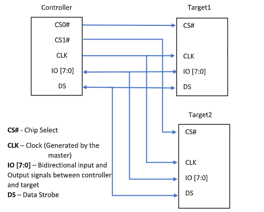
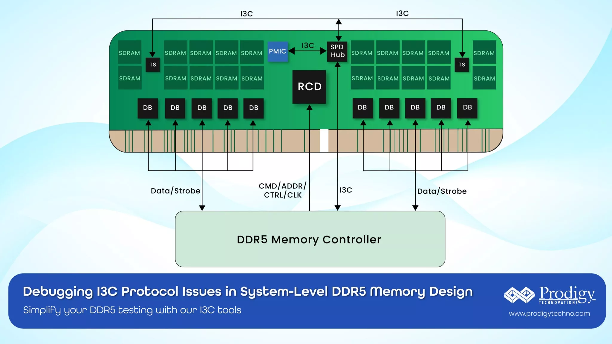
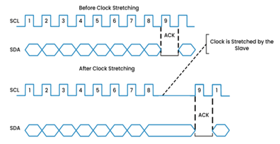
The I3C protocol supports several communication formats, all utilizing a two-wire interface. The two wires are designated as SCL and SDA. SDA is a bi-directional data pin, while SCL can either serve as a clock pin or a bi-directional data pin in certain HDR modes.

All I3C communication occurs within a frame, beginning with a START condition, followed by one or more transfers, and ending with a STOP condition. The I3C interface supports Single Data Rate (SDR) messages, similar to I2C messages, with a maximum clock speed of 12.5 MHz. It also supports High Data Rate (HDR) messages, where data transfer is synchronized with clock cycles. There are two types of messages: Broadcast and Direct Common Command Code (CCC) messages, allowing the master to communicate with all or specific slaves on the bus.

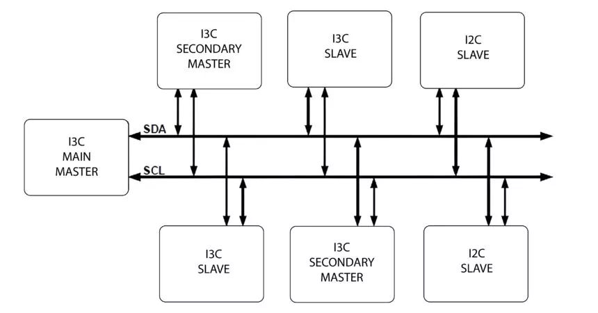
Figure 1: I3C Bus Diagram

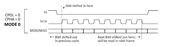
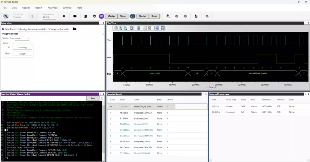
I3C protocol is based on frame encapsulation approach. The I3C frame always include START, the Header, the data and the STOP. I3C bus always initialized in SDR mode and never in HDR modes. Common Command Code (CCC) commands protocol is formatted using only in SDR. CCC are transmitted to specific to slave or all slaves in I3C bus. CCC General format as shown in this figure.

At start up stage from power-down, main master shall assign unique dynamic address to every device on the bus including itself. Dynamic address creates a priority ranking of device interrupts. If any secondary master present in the I3C bus shall be made aware of dynamic address and characteristic registers. For more details on I3C protocols, please refer to MIPI® I3C specifications.

PGY-I3C-USB-ADT Applications

Use Cases for PGY-I3C-USB-ADT in Manufacturing

  • Production Line Testing: Diagnose communication errors between I3C masters (controllers) and slave devices (sensors) during assembly, identifying faulty components or configuration

Key Considerations for Implementing PGY-I3C-USB- ADT

  • API Integration: Opt for analyzers with API functions the user can create test automation for efficient data capture, analysis, and
  • Support application frequency range as per I3C Spec, Commands, configurable as controller (master) or target (Slave)

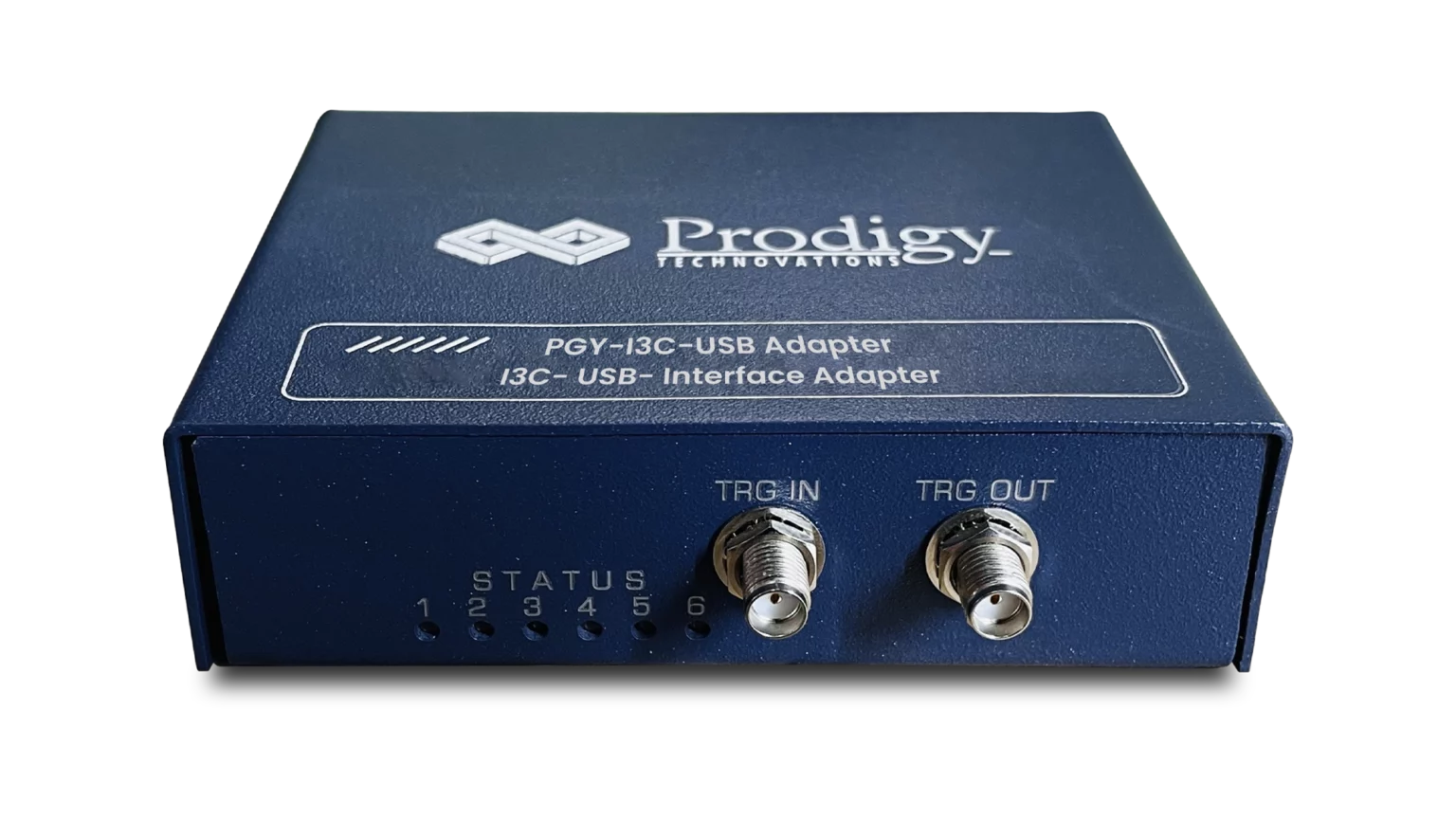
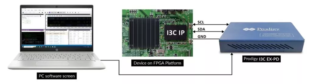
         Figure 2: PGY-I3C-USB-ADT Hardware Device

Testing a  I3C Master or Slave:

I3C DUT can be Master or slave. The API script runs in the host computer through any API environment can initiate I3C Traffic and response through the same. User can set up the Master or Slave characteristic registers of PGY- I3C- USB-ADT based on the requirement in DUT by Configuring the functions by modifying the API Script.


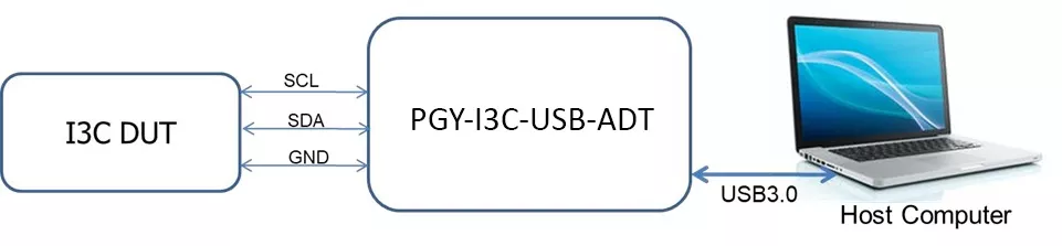
Figure 3:PGY-I3C-USB-ADT Test Setup

Using the API Script in PGY-I3C-USB-ADT software designers can initiate the communication with DUT. For example, user can send ENTDAA command which is instantiation command during the power up state. By running this API script Master (in this case PGY-I3C-USB- ADT) sends the commands to DUT.

Script forconfiguring Master and Slave:

if exercise.EstablishConnection() == eResponseFlag.Success: #Connection Establishment

print (“Connection Successful”) “””response = exercise.ResetAll() print”reset done”

time.sleep(1)

response =exercise.EstablishConnection()”””

response = exercise.AddNode(eNodeType.Master, 1.8) #Add Master

ifresponse == eResponseFlag.Success: print(” Master Added Successfully “) response =

exercise.AddNode(eNodeType.I3C_Slave,1.8,”6b”,0x208

006c900b,0x26,0,eDeviceType.Internal,eTerminationTyp e.ON,255) #Adding Slave(eNodeType,Voltage,”Static address”,PID,BCR,DCR,Interface,termination,255)

ifresponse == eResponseFlag.Success:

print(” Slave with Node ID= 1 addedsuccessfully “) response = exercise.StartCapture()

ifresponse == eResponseFlag.Success: print(” Capture Started”)

Once thecapturestarts, we willthen emulatethe I3C bus configuration.

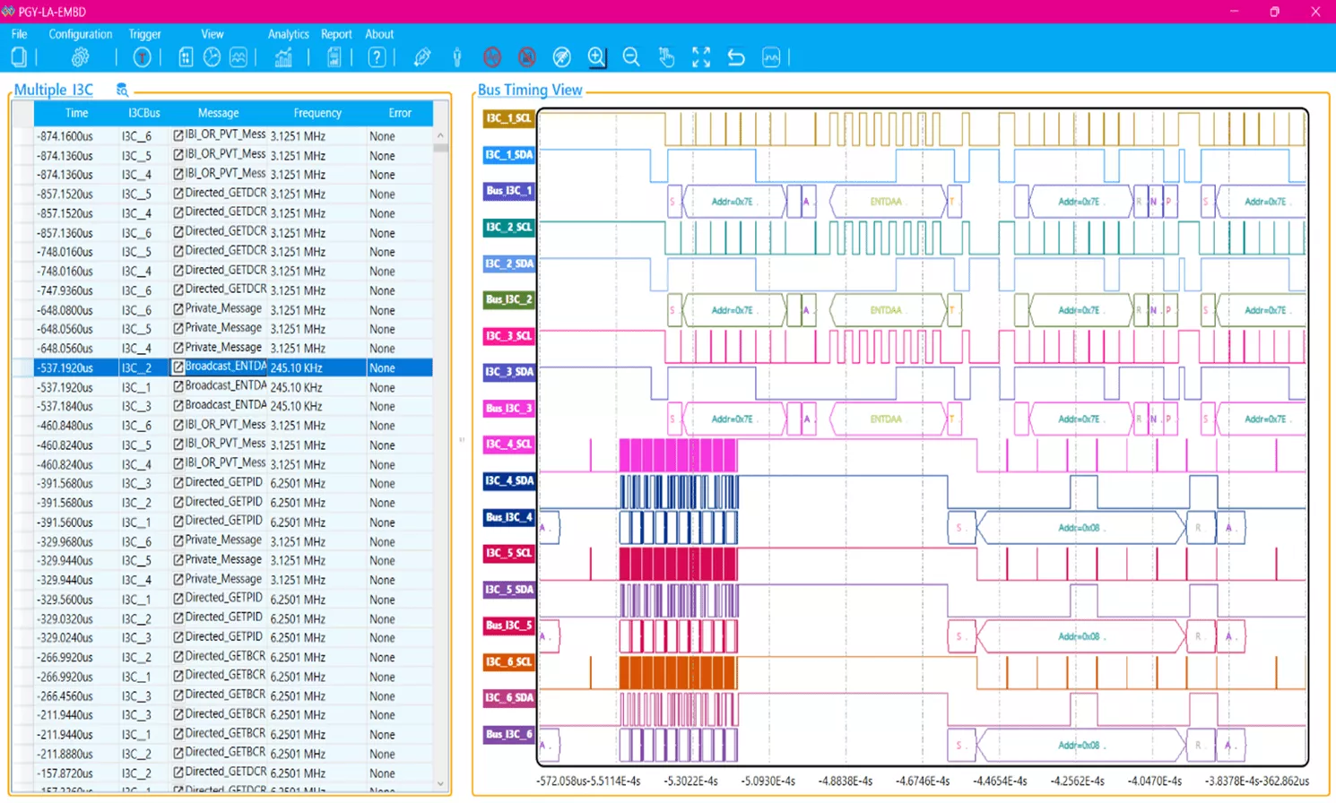
In real world, I3C devices are expected to work in I3C bus configuration. Where there will be main master, I3C Slave. Hence it is important for design and test engineer to test the I3C devices in I3C Bus configuration.

PGY-I3C-USB-ADT can be configured has single master, single slave to address the need of emulating I3C Bus. User can setup the different characteristic registers of I3C devices in PGY-I3C-USB-ADT and configure the I3C Busalong with DUT.

We instantiate the I3C bus by sending ENTDAA command so that addresses are assigned and then we didwriteand readthedatafrom I3CSlave.

Scriptfor ENTDAA :

defloadScriptENTDAA():

response = exercise.FormMessageMaster(eFrameType.BROADCA ST,0,eTransferType.Read,9,[0],True,0x07)

ifresponse !=eResponseFlag.Success: print(exercise.GetResponseDescription(response))

else:

print(“ENTDAA sent successfully”)

Once after assigning the Dynamic address to the I3C slave, we are performing Private write and read operation to the slave using the private write and read commands.

Script for Private Writeand Read :

def Pvt_wr():

response                                                          =

exercise.FormMessageMaster(eFrameType.PRIVATE,1,eT ransferType.Write,0,[0x0f, 0x08, 0x09, 0x0A],False)

print(“Response Pvt_wr:”,response)

if response != eResponseFlag.Success:

print (exercise.GetResponseDescription(response)) else:

print (“Pvt_wr”) def Pvt_rd():

response =

exercise.FormMessageMaster(eFrameType.PRIVATE,1, eTransferType.Read,4,[0],True)

print(“Response Pvt_rd:”,response)

if response != eResponseFlag.Success: print(exercise.GetResponseDescription(response))

else:

print(“Pvt_rd”)

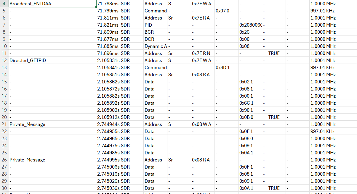
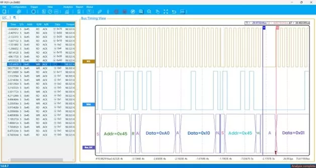
Figure 5: Report generated from the results

Once the script is run, the I3C-USB-ADT will generate a .csv file along with all the details such as frequency, time stamp, address, data , errors and save it in a defined path. This allows the user to easily verify test scenarios in the future by reviewing the report. Using scripting language user can compare the test results with golden reference data and decide pass/fail condition of the device under test.

The PGY-I3C-USB-ADT supports emulating and verifying all I3C commands according to the MIPI I3C specification. Configuration details for all commands are explained in the PGY-I3C-USB ADT User Manual, and users have the provision to write their own automation scripts for specific test scenarios.

Prodigy Technovations  also offers a range of I3C protocol products, including the PGY-I3C-EX-PD (I3C Exerciser and Protocol Analyzer), which is characterization of I3C interface for protocol and timing performance in pre an dpost silicon validation environment. It is also an efficient too to debug the design issues in failed devices.

Additionally, Prodigy Technovations provides oscilloscope-based electrical validation software(PGY-I3C-EV-PD) for the I3C electrical  parameter verification for open- drain and push-pull frequencies.

Another notable product is the PGY-I3C-EX-PD Lite, similar to the PGY-I3C-USB-ADT, but it includes GUI and API support for automation scripting. This tool addresses needs of application engineering team needs or application where you donot need to vary the timing and amplitude parameters as well not large test cases.

For more details about the range of I3C products, you can visit Prodigy Technovations.

Conclusion

I3C protocol analyzers are essential for manufacturers aiming to enhance product quality, optimize production efficiency, and streamline development processes. These analyzers offer comprehensive insights into I3C communications within devices, leading to a more dependable and robust production environment.

The industry-leading PGY-I3C-USB-ADT provides a powerful verification solution to address the testing challenges of I3C devices, including controllers and targets. In large chip and chipset manufacturing companies, the PGY-I3C-USB- ADT plays a significant role in product testing. It generates I3C protocol packets per I3C V1.0 (upgradable for upcoming specifications), offering a reference I3C device for comparative analysis and debugging.

Overview

In the realm of embedded systems, I2C (Inter-Integrated Circuit) is a widely used communication protocol that enables devices to communicate with each other over a short distance. One critical aspect of I2C communication is clock stretching, which allows slower devices to control the pace of communication by holding the clock line low. One of the challenge for design engineer to monitor the infrequent clock stretching event while multiple I2C connected in the bus. Which device is stretching the clock and how it is affecting the performance of the embedded system.

The PGY-LA-EMBD, a high-performance logic analyzer, offers advanced features for analyzing I2C signals, including pulse width triggering of clock stretching. This document provides an overview of how pulse width triggering on clock stretching can be achieved using the PGY-LA-EMBD logic analyzer.

Clock Stretching in I2C

Clock stretching is a mechanism used in I2C communication where a slave device can hold the SCL (clock line) low to signal the master to wait before continuing communication (as illustrated in Figure1). This ensures data integrity when the slave needs more time to process information. The master device must wait until the slave releases the SCL line before resuming communication. This feature is particularly useful when the slave requires extra time for processing, buffering, or synchronization, but it does require the master to support clock stretching for the communication to proceed correctly.

Figure 1: I2C Clock Stretching

Pulse Width Triggering

Pulse width triggering is a powerful feature in logic analysers that allows users to capture events based on the duration of a pulse. In the context of I2C clock stretching, this feature is particularly useful for detecting and analysing instances where the clock line (SCL) is held low for clock stretching to by the device in a i2C since this device needs more time to respond. In an I2C bus, not all devices will equal response time. Though I2C bus may work 10Kbps speed, to capture infrequent event of clock stretching in an logic analyser or I2C analyser is difficult. The pulse width triggering enables the capturing of this event by setting pulse width trigger by setting pulse width more than 100Kbps data rate. This capability helps engineers identify timing issues, performance bottlenecks, and other anomalies in I2C communication.

The PGY-LA-EMBD offers various triggering options, including pattern triggers, protocol-aware triggers, and timing parameter triggers. The timing parameter trigger, a form of pulse width triggering, allows users to set the pulse width on the negative edge. This means the PGY-LA-EMBD will trigger on the negative edge if the clock line stays low longer than the specified pulse width.

Figure 2: Pulse width trigger setting on PGY-LA-EMBD

For example, in Figure 2, the pulse width triggering is configured with a pulse width greater than 10,000 ns on the negative edge. In this example, the I2C signal is captured with a frequency of 100 kHz and a period of 10,000 ns. At some instances, clock stretching occurs, and the pulse width triggering feature in the PGY-LA-EMBD is used to capture these events accurately.

Figure 3: waveform captured for I2C Clock stretching

Figure 3 illustrates an I2C waveform during a write-read transmission. After the read transmission, the clock is stretched during the write message, resulting in a clock stretching event lasting 30,000 ns. Vertical cursors are used to measure the duration of this clock stretching. Clock stretching occurs when the I2C slave device holds the clock line (SCL) low, temporarily pausing communication to process data. In this example, the PGY-LA-EMBD logic analyzer is configured to trigger on clock stretches longer than 10,000 ns to capture this infrequent event. When this threshold is exceeded, logic analyzer with I2C decoding capability will notify the trigger point is marked with a “T” on the bus view, making it easy to identify and analyse the delay. This setup helps diagnose timing and performance issues in I2C communication, ensuring reliable operation.

Conclusion

Pulse width triggering of clock stretching on I2C using the PGY-LA-EMBD logic analyzer with I2C decoding capability provides a robust method for analysing and troubleshooting I2C communication. By leveraging the advanced triggering capabilities of the PGY-LA-EMBD, engineers can gain deeper insights into the timing behaviour of their I2C systems, ensuring reliable and efficient communication in their embedded applications.

Request For Quote

Share your requirement and our team will provide a tailored quote based on your validation needs.

"*" indicates required fields

This field is for validation purposes and should be left unchanged.
Address*

Request For Demo

Tell us your use case and our team will schedule a product demo aligned to your validation workflow.

"*" indicates required fields

This field is for validation purposes and should be left unchanged.
Address*

Request A Demo

Tell us your use case and our team will schedule a product demo aligned to your validation workflow.

"*" indicates required fields

This field is for validation purposes and should be left unchanged.
This field is hidden when viewing the form
Address*

Request Quote

Share your requirement and our team will provide a tailored quote based on your validation needs.

"*" indicates required fields

This field is for validation purposes and should be left unchanged.
Address*